

Flex PCB Design: Guide to Achieving Optimal Performance
Flex PCBs (Flexible Printed Circuit Boards) have gained significant popularity due to their versatility, compactness, and ability to withstand complex design requirements. These flexible circuits are used in a wide range of industries, from consumer electronics to aerospace and automotive applications. To ensure optimal performance and reliability, it is crucial to understand the requirements and best practices for designing flex PCBs. In this blog, we will explore the essential aspects of flex PCB design and provide a comprehensive guide to achieving optimal performance.
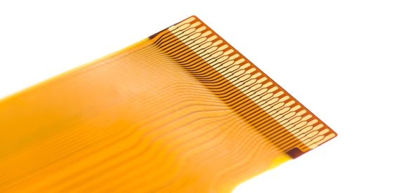
I. Understanding Flex PCBs: A Brief Overview
Flex PCBs, also known as flex circuits or flexible printed circuits, are electronic interconnects created from flexible plastic substrates. Unlike rigid PCBs, these flexible circuits offer the advantage of bending, twisting, or folding, enabling them to conform to non-planar surfaces or fit into compact spaces. Flex PCBs consist of a flexible substrate material with conductive traces and components mounted directly onto it, eliminating the need for separate connectors and cables.
II. Design Considerations for Optimal Flex PCB Performance
1. Flexible Substrate Selection:
The choice of substrate material is critical in flex PCB design. Common materials include polyimide (PI) and polyester (PET), known for their excellent flexibility, thermal stability, and dielectric properties. The selection should consider factors such as temperature requirements, flexibility, and overall performance of the circuit.
2. Bend Radius and Flexibility:
The bend radius determines how tightly the flex PCB can bend without causing damage to the conductive traces or components. Designers should adhere to the manufacturer’s recommended bend radius to ensure the integrity of the circuit. Additionally, understanding the flexibility requirements of the application helps in selecting the appropriate substrate thickness and reinforcement options.
3. Trace Routing and Placement:
Proper trace routing and component placement are crucial for optimal signal integrity and electrical performance. Designers should avoid sharp bends and acute angles in the traces, as they can lead to signal loss or breakage. Placing sensitive components away from areas with high mechanical stress helps prevent damage during flexing or bending.
III. Manufacturing Guidelines for Flex PCBs
1. Stacking Order:
The stacking order of a flex PCB refers to the arrangement of layers, including conductive layers, dielectric layers, and cover layers. Understanding the stacking order is vital to ensure proper functionality and mechanical integrity. Collaborating with manufacturers, such as Winow New Energy Company, enables designers to optimize the stack up for their specific application.
2. Fiducial Marks and Alignment:
Incorporating fiducial marks during the design phase helps achieve precise alignment during manufacturing. These marks enable accurate registration of layers, ensuring proper placement of vias, pads, and components. Proper alignment enhances reliability and reduces the risk of manufacturing defects.
3. Via Placement and Reinforcement:
Vias are essential for establishing connections between different layers of a flex PCB. Careful consideration should be given to via placement, as they can impact the flexibility and reliability of the circuit. Reinforcing areas around vias and high-stress points helps distribute mechanical strain and enhances the overall durability of the flex PCB.
IV. Testing and Validation
1. Electrical Testing:
Before finalizing the design, electrical testing is crucial to ensure signal integrity, impedance control, and the absence of shorts or opens. Rigorous testing, including continuity checks, resistance measurements, and high-frequency signal integrity analysis, should be performed to identify and rectify any potential issues.
2. Flexing and Fatigue Testing:
Flex PCBs are subjected to repetitive flexing and bending in many applications. Conducting flexing and fatigue testing helps evaluate the endurance and reliability of the design. By simulating real-world operating conditions, designers can identify weak points and make necessary adjustments to improve the overall performance and lifespan of the flex PCB.
Ⅴ. Flex PCB Design: Innovative Solutions for Modern Electronics
Flex PCBs have revolutionized the field of electronics with their unique ability to bend, twist, and conform to various shapes and contours. These versatile circuit boards offer a multitude of benefits, making them an ideal choice for modern electronic devices.
1. Flex PCB Design Advantages:
Flex PCBs provide several advantages over traditional rigid circuit boards. Firstly, their flexibility allows for space-saving in compact electronic devices, enabling designers to create smaller, lighter, and more streamlined products. Additionally, the ability to bend and flex enables easier integration into three-dimensional and irregularly shaped surfaces, providing greater design flexibility.
2. Enhanced Durability and Reliability:
Flex PCBs are built to withstand the demands of today’s dynamic electronics industry. Their flexible nature allows them to endure repeated bending and twisting without compromising performance, making them highly durable. With the reduction of interconnects and solder joints, the risk of mechanical failure and signal loss is significantly minimized, resulting in improved reliability for electronic devices.
3. Applications in Various Industries:
Flex PCBs find applications in diverse industries, including consumer electronics, automotive, aerospace, medical devices, and more. In consumer electronics, they are used in smartphones, wearables, and tablets, where space and flexibility are crucial. In the automotive sector, Flex PCBs enable the integration of advanced features, such as touchscreens, sensors, and adaptive lighting systems. The aerospace industry benefits from their lightweight nature and ability to withstand harsh environments, while the medical field relies on Flex PCBs for flexible circuits in devices like pacemakers and medical imaging equipment.
4. Miniaturization and Component Density:
One of the key advantages of Flex PCB design is its ability to accommodate a higher component density. By utilizing advanced manufacturing techniques, such as laser drilling and micro via technology, smaller and more intricate circuits can be realized. This miniaturization not only enables the development of smaller devices but also facilitates the integration of complex functionality within limited space, leading to more advanced and feature-rich electronic products.
Conclusion:
Designing flex PCBs requires a thorough understanding of the unique considerations and best practices associated with flexible circuits. By carefully selecting the substrate material, optimizing trace routing, and collaborating closely with manufacturers, such as Winow New Energy Company, designers can achieve optimal performance, reliability, and longevity in their flex PCB designs. Implementing proper manufacturing guidelines, testing, and validation processes ensures that the flex PCB meets the application’s requirements and performs flawlessly in demanding environments. With the right approach, flex PCBs offer unparalleled flexibility and compactness, empowering the development of innovative and advanced electronic devices.