

How Many Layers Can a PCB Have and What Are the Benefits of Each Layer?
Printed circuit boards (PCBs) are the foundation of almost all electronic devices. They are complex electrical systems, consisting of many layers of material and components. But how many layers can a PCB have? And what are the benefits of each layer? With the help of modern technology, PCBs can now be made with up to 20 layers, allowing complex designs and components to be packed into a small space. Each layer has its own purpose, from providing power to the components to controlling signal paths and ensuring the board is properly insulated. With careful consideration, designers can take advantage of the unique benefits of each layer in order to create efficient and reliable circuits. Whether you’re a beginner or a seasoned engineer, understanding how each layer contributes to the overall design is essential for successful PCB fabrication.
What is a PCB?
A printed circuit board (PCB) is a flat, rigid board with a pattern of holes drilled into it. It is normally made of fiberglass, epoxy resins, or a synthetic polymer. A PCB is used to make an electrical circuit on a smaller and more flexible surface than a breadboard or printed wiring board. Circuits are built on a single PCB by routing the electrical components, such as resistors, capacitors, and integrated circuits (ICs), and connecting them together with copper wires that are soldered to the terminals or leads of the components. PCBs are used in most electrical and electronic equipment, such as computers, televisions, space vehicles, medical diagnosis equipment, and many other types of equipment. PCBs can have many layers and many different functions. The top layer, or surface layer, is usually in an epoxy resin that is laminated to a fiberglass fabric. This surface layer is usually copper-coated, and it is electroplated with a thin layer of nickel. The nickel is used to make soldering the components easier, and it provides the necessary insulation between the copper core and the parts being soldered.
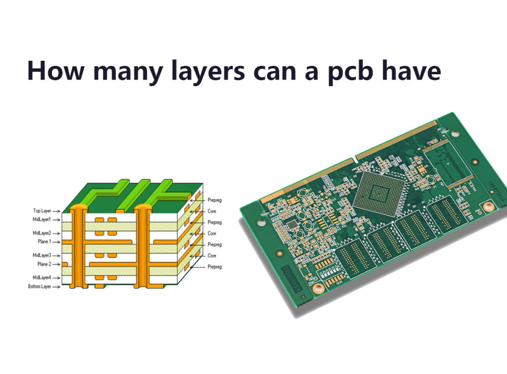
How Many Layers Can a PCB Have?
The number of layers in a PCB is not set in stone. While you may go into your project knowing you’ll need a single-sided board with a specific number of layers, the design process can take you in many different directions. It’s important to be flexible, especially when you’re working on a large-scale project that holds great significance for an organization or industry. You never know where your research will lead you—the more you know, the better equipped you’ll be to create a functional circuit that is reliable and efficient. When choosing the number of layers in your circuit board, the most important thing is to make sure each layer has a specific purpose. A design with too many layers can get confusing, while a design with too few layers will not function properly. It’s also important to consider the thickness of each layer, as thicker layers require more time and effort to fabricate.
What are the Benefits of Each Layer?
The first layer of a PCB design is often referred to as the surface layer, or the top layer. This layer contains the components that are visible on the outside of the board. It’s also where traces are routed to connect these components. Because this is the top layer of the board, the surface layer must be a durable material that can withstand impact and other environmental factors, such as water and chemicals. The ground layer, also known as the, “back side” or “backplane,” is the other end of the board that is not visible from the outside of the board. This layer is essential for ending all the electrical connections. It provides a pathway for current to flow through the board without becoming “electrically noisy.” The ground layer must be connected to a common ground so that all the components are properly grounded.
Layer 3: The Signal Layer
The signal layer is where you place your traces and components that are responsible for routing electrical signals. This layer should be as thin as possible so that it does not add unnecessary weight or thickness to the board design. The signal layer should also be stiff enough to prevent bending and warping. There are many ways to route signals, such as through-hole, through-hole mounting, surface mount, or edge mount. The surface mount technique is often used in high-density circuits because it is less affected by changes in temperature.
Layer 4: The Power Layer
The power layer is responsible for supplying power to the components and traces on the PCB. This layer is usually thicker than the other layers, especially if it needs to be able to withstand high voltages. The power layer is often found on the bottom or middle of the PCB board, which is why it’s important to plan your designs with component placement in mind. The power layer is also where designers will place any decoupling components, such as capacitors, that are responsible for reducing noise in the circuit.
Layer 5: The Insulation Layer
The final layer in your PCB design is the insulation layer, which protects all the other layers from being shorted. The insulation layer is usually made of a material that is not easily shorted out, such as polyimide film or polyester. This layer is usually where the design is cut out, but the area underneath the cut lines is also insulated to prevent short circuits. When choosing the number of layers in your circuit board, the most important thing is to make sure each layer has a specific purpose. A design with too many layers can get confusing, while a design with too few layers will not function properly. It’s also important to consider the thickness of each layer, as thicker layers require more time and effort to fabricate.
Conclusion
A printed circuit board (PCB) is a flat, rigid board with a pattern of holes drilled into it. It is normally made of fiberglass, epoxy resins, or a synthetic polymer. A PCB is used to make an electrical circuit on a smaller and more flexible surface than a breadboard or printed wiring board. Circuits are built on a single PCB by routing the electrical components, such as resistors, capacitors, and integrated circuits (ICs), and connecting them together with copper wires that are soldered to the terminals or leads of the components. PCBs are used in most electrical and electronic equipment, such as computers, televisions, space vehicles, medical diagnosis equipment, and many other types of equipment.