

PCB Design and Assembly For Your Business
Here are the general steps involved in PCB design and assembly:
- Design: The first step in PCB design is to create a schematic diagram, which is a graphical representation of the circuit and its components. This step typically involves software tools such as computer-aided design (CAD) software.
- Component selection: The next step is to select the components that will be used in the circuit. This may include components such as transistors, capacitors, resistors, and integrated circuits.
- Prototyping: Once the design is complete, a prototype PCB is typically built to verify that the circuit functions as intended. This may involve creating a PCB layout using CAD software and manufacturing the prototype using photolithography and etching techniques.
- Testing: The prototype PCB is tested to ensure that it functions properly and meets the required specifications. Any defects or issues are identified and corrected.
- Mass production: If the prototype PCB is successful, the design is finalized and the PCB is mass-produced using automated assembly processes.
Overall, the process of PCB design and assembly requires a combination of technical skills and knowledge of electronics and manufacturing processes. It is an important step in the creation of electronic systems and devices, and requires careful attention to detail to ensure that the finished product is reliable and meets the required specifications.
The world of Printed Circuit Boards (PCBs) is an exciting one that is filled with potential. From PCB design and assembly to troubleshooting and manufacturing, the possibilities are endless. In this blog post, we will explore the world of PCBs, their benefits, design, assembly, components, types, and tools. We will also provide you with tips and resources to help you unlock your PCB design and assembly potential. So let’s get started!
What is a Printed Circuit Board (PCB)?
A Printed Circuit Board (PCB) is a board made of non-conductive material, typically fiberglass, on which the electrical components of an electronic device are mounted. PCBs are used in a wide variety of applications, from computers to televisions to medical equipment. They provide a reliable, cost-effective way to connect and control the electrical components of an electronic device.
PCBs are made up of copper traces, which are thin copper lines that connect different components on the board. These traces are then covered with a layer of solder mask, which is an insulating material that prevents short circuits and prevents any corrosion. The components are then mounted on the board using soldering or surface mount technology.
Benefits of PCB Design and Assembly
There are a number of benefits to using a PCB design and assembly process. One of the biggest benefits is that it is a cost-effective way to produce electronic devices. With PCBs, you can reduce the cost of individual components, as well as the cost of manufacturing.
Another benefit of PCB design and assembly is that it is a reliable way to connect and control the electrical components of an electronic device. By using a PCB, you can reduce the number of errors that can occur during the manufacturing process. This can help to ensure that the electronics are functioning properly.
Finally, by using a PCB design and assembly process, you can reduce the amount of time it takes to manufacture an electronic device. This can help to reduce the time to market for a product and allow for more efficient production.
PCB Design and Assembly Process
The PCB design and assembly process typically involves a number of steps. First, the components for the PCB must be selected and ordered. Next, the components are placed on the board and soldered in place.
Once the components are in place, the board is tested to ensure that all the components are functioning properly. This is done using a test fixture, which is a device that connects the components to a power source. Once the board has been tested, it can then be assembled into a finished product.
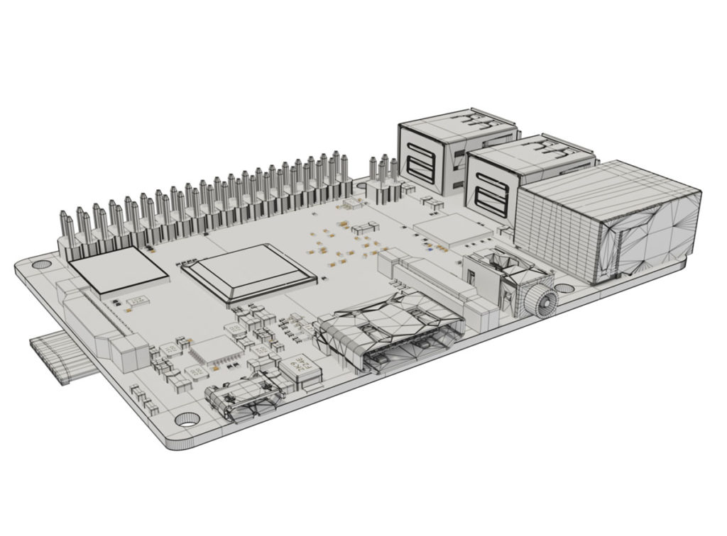
Components of a PCB
A PCB typically consists of several components, which include the board, the copper traces, the solder mask, and the components. The board is made up of a non-conductive material, such as fiberglass, on which the electrical components are mounted. The copper traces are thin copper lines that connect different components on the board. The solder mask is an insulating material that prevents short circuits and prevents any corrosion. Finally, the components are the actual electrical components that are mounted on the board.
Types of PCBs
There are a number of different types of PCBs, each of which is designed for a specific application. Single-sided boards are the most common type of PCB and are used for simple circuits. Double-sided boards are used for more complex circuits and allow for more components to be connected. Multi-layer boards are used for even more complex circuits and allow for even more components to be connected. Finally, flex boards are used for applications where the board needs to be bent or flexed.
Tips for Successful PCB Design and Assembly
There are a few tips that can help to ensure successful PCB design and assembly. First, it is important to choose the right components for the board. This will help to ensure that the board will function properly and will be able to withstand the test of time.
Next, it is important to plan out the design of the board before starting the assembly process. This will help to ensure that the board is laid out properly and that all of the components will be connected correctly.
It is also important to use the right tools for the job. Using the right tools, such as soldering irons and multimeters, can help to ensure that the board is assembled properly and that the components are functioning correctly.
Finally, it is important to use the proper soldering technique. This will help to ensure that the components are properly connected and that the board will work as intended.
PCB Design and Assembly Tools
There are a number of tools that are used in the PCB design and assembly process. These include soldering irons, multimeters, and pliers. Soldering irons are used to heat up the components so that they can be soldered in place. Multimeters are used to measure the electrical current of the board to ensure that it is functioning properly. Pliers are used to help manipulate the components and to ensure that they are properly placed on the board.
PCB Design and Assembly Services
There are a number of companies that offer PCB design and assembly services. These companies can help to ensure that your PCB is designed and assembled properly and that it will function as intended. Many of these companies offer a variety of different services, such as layout design, component selection, and troubleshooting.
Using a professional PCB design and assembly service can help to ensure that your project is done right the first time and that any problems are addressed quickly and efficiently.
PCB Design and Assembly Resources
There are a number of resources available to help you with your PCB design and assembly process. These include online tutorials, forums, and blogs. Online tutorials can help to provide step-by-step instructions on how to design and assemble a PCB. Forums can be used to ask questions and to get advice from experienced PCB designers and assemblers. Finally, blogs can provide helpful tips and tricks for successful PCB design and assembly.
Conclusion
PCBs are an incredibly powerful tool that can be used to create a wide variety of electronic devices. By understanding the basics of PCB design and assembly, you can unlock your PCB design and assembly potential. We hope that this blog post has provided you with the information and resources you need to get started.
So don’t wait any longer, start exploring the world of PCBs and unlock your PCB design and assembly potential today!