

Demystifying The Printed Circuit Board Assembly Process
Are you interested to know about the printed circuit board assembly process?
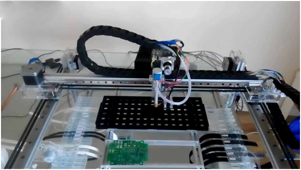
Packaging printed circuit boards (PCBs) is crucial in producing various electronic devices in electronics manufacturing. PCBs are the foundation of contemporary technology, from computers and cell phones to medical devices and automobile systems. The printed circuit board assembly process is the crucial link connecting the world of design and the physical world of electronics. The complex procedure gives life to carefully thought-out and painstakingly built PCBs, turning them into useful electrical gadgets that power our contemporary world. Electronic components are flawlessly merged into the PCB’s surface over complex stages, resulting in a functional, unified system. The intricacy of the PCB design, the kind of components utilized, and the manufacturing volume all impact the assembly process, which varies accordingly. While manual labour may be utilized for smaller quantities or prototypes, automated technology is frequently used for high-volume manufacturing.
Exploring the Composition of PCBs: Unveiling the Heart of Modern Electronics
Printed Circuit Boards (PCBs) are the essential building elements that power a wide range of devices, from cell phones to spaceships, in contemporary electronics. Despite their insignificance, PCBs are a wonder of engineering, made up of several important parts that are painstakingly combined to create circuits. In this blog article, we’ll explore PCBs structure, printed circuit board assembly process and identify the components that make up these modern marvels. Typically, it is constructed from a non-conductive substrate material like FR-4, which is fibreglass-reinforced epoxy resin. The electrical components and traces on the board are mechanically supported and insulated by the FR-4 material. Here’s a general overview of the layers and components that make up a PCB:
The Substrate Layer: The Foundation
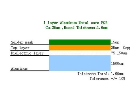
Every PCB has a substrate layer in its centre, a crucial foundation made of a substance known as FR-4. This abbreviation, “Flame Retardant 4,” refers to an epoxy resin with fibreglass reinforcement that serves as the board’s structural support and insulator. Because of its superior mechanical qualities, such as its durability, heat resistance, and dielectric qualities, FR-4 is the material of choice for making PCBs.
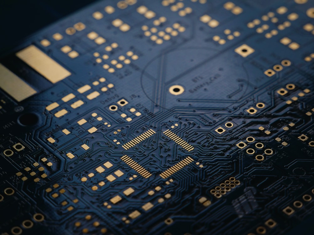
Copper Foil: Conductive Pathways
Copper foils are laid on top of the substrate layer, and each is carefully glued to the board’s surface. These copper layers act as a complicated network of conductive lines connecting various components to allow the transmission of electrical impulses. Copper is the best material for transferring data and power across the PCB because of its high electrical conductivity and solderability.
Protecting Against mishaps: Solder Mask
Have you ever wondered what the green coating on PCBs is for? That is the solder mask, a covering that protects the copper lines beneath from accidental contact, corrosion, and the effects of the environment. The solder mask is made of epoxy-based polymers and created using photolithography, leaving just the portions intended for soldering exposed. It is impossible to stress the importance of this layer in preventing shorts and preserving signal integrity.
Hands-on: Silkscreen Layer
The PCB’s visual storyteller is the silkscreen layer, which uses non-conductive ink to print critical information like component designators, logos, and reference points. This white layer helps technicians with component placement, identification, and assembly while also improving the board’s aesthetics and functionality. The unsung hero who makes sure that circuit realization is exact.
Vias: Seamless Connections
Think of a multi-story structure with stairs linking the various levels. Similar functions are carried out by vias in printed circuit boards (PCBs), which join several levels of the board to enable vertical signal transmission. The utility and intricacy of the board are increased by these tiny, plated holes that allow for smooth connection between layers. Visas are available in a variety of kinds, including through-hole vias and micro vias, to meet diverse design needs.
Constructing blocks: Components
Any PCB’s constituent parts—from sophisticated microprocessors to resistors and capacitors—make up its fundamental character. The functional centre of the circuit is formed by these parts, which are soldered onto the board’s surface. The performance and dependability of the finished electronic equipment are directly influenced by the accuracy of their positioning, alignment, and soldering.
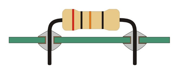
Solder joints: Solidify connections
The metallic connections between components and copper traces, known as solder joints, cement the circuit’s links. A strong connection is created when a solder alloy is heated until it melts and cools. The durability of the PCB is directly impacted by the quality and strength of these joints, guaranteeing a durable and reliable connection throughout time.
The design of PCBs continues to be a pillar of innovation in the ever-changing world of technology. PCBs embody the art and science of electronics, from their fibreglass-reinforced substrate layer to the painstakingly created copper traces and components. Understanding the complex elements that make up these circuitry marvels helps us better grasp the electronic world’s secrets as we continue to push the boundaries of what is possible.
A Deeper Dive into the Printed Circuit Board Assembly Process:
- Modern technology is expanding the world at a very rapid rate, and its impacts are easily seen in our day-to-day activities. Our way of life has altered significantly. Many advanced pieces of equipment have entered the globe thanks to technical advancements that we could not have predicted ten years ago. Electronics engineering is at the heart of this machinery, and printed circuit boards (PCBs) serve as its foundation.
- The components, the copper layer that creates the traces, the holes into which the components are inserted, and layers that may be inner or outer layers make up the PCB. The substrate is constructed of fibreglass. RayPCB can produce up to 1-36 layers for multilayer PCB prototypes, and for multilayer PCB mass production, we can deliver 1-10 layers. The outside layers are there, but there is no inside layer on single-sided and double-sided PCBs.
- The rigid body that houses numerous electrical components is known as the PCB, which is typically green in colour. The “PCB Assembly” or PCBA procedure involves soldering these parts to the PCBs. A PCB goes through several complex phases, from the initial design to the finished product, necessary for a successful assembly. In this blog article, we will walk you through each step of creating a PCB.
PCBs, or printed circuit boards, are the heroes that support the operation of almost every electronic gadget we use on a daily basis. Beyond just joining components together, PCBs are at the centre of several applications that span various sectors and technological advancements. In this blog article, we examine PCBs’ many uses in more detail, highlighting how vital they are to the functioning of contemporary society.
- Consumer Electronics: From Smartphones to Smart Homes
The complex interaction of PCB s essential to the success of consumer electronics, including smartphones, computers, TVs, and wearable technology. These small boards make the integration of microprocessors, memory modules, sensors, and communication chips possible, enabling seamless interactions between people and technology. Additionally, PCBs are the driving force behind the emerging smart home trend, where they manage everything from security systems to lighting and thermostats, enhancing efficiency and ease.
- Automotive Innovations: Moving Quickly and Accurately
Electronics have sparked a revolution in the automobile sector, and PCBs are at the forefront of this change. In contemporary automobiles, PCBs operate the engine, safety features, infotainment screens, navigational devices, and advanced driver assistance systems (ADAS). Through real-time data processing and transmission, these boards improve vehicle performance and contribute to safety.
- Healthcare Innovations: High-Tech Healing
PCBs have made it possible for healthcare to make improvements that have saved many lives. Precision electronics are integrated into PCBs, which are used in diagnostic devices like MRI and CT scanners and wearable health monitors to give precise diagnoses, therapy delivery, and patient monitoring. Telemedicine and minimally invasive surgery have been made possible by PCBs’ dependability and miniaturization, revolutionizing patient care.
- Networks of Communication: Linking the Global Village
Huge communication networks are the backbone of our linked world, and PCBs are the workhorses that make it possible. These boards control data flow, enhance signal quality, and guarantee continuous connectivity in cell towers, routers, switches, and satellites. The requirement for higher data speeds, reduced latency, and wide coverage is still driving PCB advancements in the telecommunications industry.
- Industrial Automation: Scaled Precision
Precision and automation made possible by PCBs benefit a wide range of industries. PCBs are used by industrial sensors, robots, control systems, and manufacturing processes to regulate operations, keep track of equipment health, and maximize productivity. PCBs are crucial to the Fourth Industrial Revolution’s (Industry 4.0) adoption in the industrial landscape because they enable smart factories and efficient manufacturing.
- Exploring the Universe: Aiming for the Stars
PCBs are crucial to space exploration efforts far beyond our planet. Spacecraft, satellites, and rovers need powerful electronics that withstand harsh environments. The complex control and communication systems that support space missions gathering information from far-off celestial bodies, and transmitting it back to Earth, are made possible by PCBs.
Have you ever wondered how a printed circuit board (PCB) is made?
It’s simple to take the complicated machines that run our lives for granted in our continuously changing technological environment. The printed circuit board assembly process is the basis for all these modern technical wonders, from smartphones to smart home appliances. A PCB is the unsung hero who conducts the symphony of electrical components, ensuring the smooth operation of modern devices. It is frequently concealed under layers of stylish housing. But have you ever considered the precise procedure for making these fundamental parts? Bring your gadgets to life as we take you on a tour through the intriguing world of PCB manufacturing.
- Stencil Application for Solder Paste
The printed circuit board assembly locations where the components would fit are where we first apply the solder paste. The stainless-steel stencil is covered with solder paste to accomplish this. The PCB and stencil are attached to a mechanical device, and the applicator then uniformly spreads solder paste across the board’s holes. Spreading the solder paste evenly is done by the applicator. So the appropriate amount of solder paste must be applied with the applicator. The paste will stay in the intended PCB locations after removing the applicator. The solder paste is grey in colour and is lead-free. It is comprised of 96.5% tin, 3% silver, and 0.5% copper.
- Design Verification: The Modification of the Blueprint
A thorough design verification step precedes the assembly process. Engineers carefully examine every connector, pad, and component location on the PCB layout to make sure they comply with the design requirements. Before the board enters the physical world, it is crucial to carry out this stage to anticipate future problems and enhance the board’s operation.
- Purchasing Components: Sourcing the Stars
When the design is approved: finding the required electronic parts is essential. The selection procedure is like assembling a diverse ensemble for a theatre masterpiece, with components ranging from resistors and capacitors to microprocessors and memory modules. Each component must adhere to exacting quality standards and fulfil the electrical and mechanical specifications of the design.
- Through-Hole Assembly vs SMT: The Technique Choice
The two main methods for attaching components on a PCB are Surface Mount Technology (SMT) and through-hole assembly. With SMT, microscopic components are attached directly to the board surface, enabling denser and more compact designs. Contrarily, with through-hole assembly, component leads are inserted into the board’s pre-drilled holes and soldered from the back. Determining which method to use depends on design complexity, board size, and component type.
- The Building Depth of Layers
Modern PCBs almost seldom have one dimension; instead, they include layers that resemble a complicated sandwich. Multiple core substrates are stacked throughout the layering process, each having copper foil adhering to its surface. Then, these layers are compressed and heated together to create a cohesive entity. The circuitry’s intricacy and the board’s expected functionality determine the number of layers.
- Unveiling the Design via Etching
During the etching process, the beauty of PCB manufacture really comes to life. The board’s surface is covered with a photoresist layer, and the Gerber file—a digital representation of the design—is used to expose particular photoresist regions to light. Following development, these exposed regions provide a barrier that protects the desirable copper traces from the etching agent. The numerous paths that make up the circuit are left behind once the unshielded copper has been destroyed.
- Mounting a component: Placing the Stars.
It’s time to populate the PCB with its electronic components after the copper paths have been etched into position. Resistors, capacitors, integrated circuits, and connectors are tiny wonders meticulously put onto the appropriate pads. Accuracy and steadiness are essential since even a small misalignment might result in improper connections and malfunctioning circuit boards.
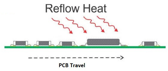
- Using solder: The Fusion
Soldering creates the links between components and copper traces in a manner similar to how a blacksmith melts metal to produce a powerful sword. The joints are coated with molten solder, a metal alloy with a low melting point. The component and copper trace are then connected safely and conductively using heat. Trained experts, there are many different soldering techniques, including reflow and hand soldering.
- Testing and Inspection: Ensuring Excellence
A PCB must complete stringent testing and inspections before it can enter the field of electronics with assurance. Technicians examine the board for problems and ensure that all connections are solid, the components are arranged correctly, and there are no obvious errors. Automated optical inspections and X-ray imaging are two cutting-edge testing techniques that assist in finding any hidden problems that can escape human examination.
- Final Touches: Coating and Finishing
A protective layer shields the fragile circuitry from environmental variables, including humidity, dust, and oxidation. This coating, typically created from a unique polymer, protects the PCB without compromising its performance. Additionally, a silkscreen layer is added to name components, connections, and other important features to improve user-friendliness and assist in troubleshooting.
- Ready for Action after deployment and packaging
The PCB has been completed and is now ready for deployment. This little, unassuming miracle is ready to power, connect, and revolutionize how we live, whether it’s a crucial component of a medical gadget, an automobile system, or the newest smartphone.
Conclusion:
The printed circuit board assembly process is a critical stage in the production of electrical devices. It entails integrating and soldering various electrical components onto a PCB to build dependable and functioning circuitry. A world-leading PCB Manufacturing and Assembly firm, RAYMING Technology, offers double-sided and multilayer printed circuit boards. winow-pcba Technology was founded in 2018. We specialize in offering high-quality PCB fabrication, PCB assembly, and component sourcing services with more than ten years of experience to worldwide businesses of all sizes. We are the PCB manufacturing assembly service provider because of our unwavering commitment to providing excellent customer service and the unmatched technical expertise of our team.