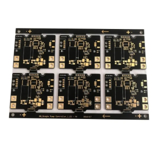
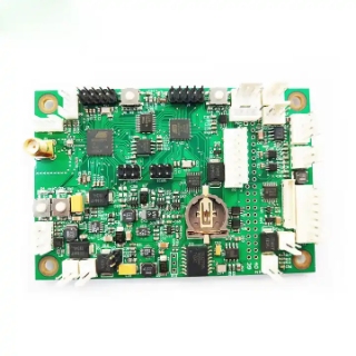
Lead Free HASLImmersion Gold PCB Double sided Printed Circuit Board PCBA
-
Supplier Type: PCB Assembly
-
Service: 24Hours Technical Services
-
Package: SMD/DIP
-
Type: PCBA
-
Brand Name: Original
-
Color: Green,Blue,Black, White, Red and more
-
MOQ: 1
- No MOQ or MPQ limited.
- Daily quotes and negotiations.
- Prototypes quotation within 3h.
- Flexible payment options.
- Prototype or mass production order acceptable.
-
Project Info
-
Specification
Guidelines for Lead-Free PCB Assembly
The lead-free PCB assembly process is divided into two fundamental parts namely, the pre-assembly process and the active assembly process. Steps involved in the lead-free PCB assembly process are detailed as follows.
Pre-assembly Steps
There are three fundamental pre-assembly steps involved in lead-free PCB manufacturing. These steps set the foundation for an error-free and precise PCB assembly. The pre-assembly steps of lead-free PCB assembly are as follows.
- Profiling:
Profiling is a prototype resembling process. The manufacturers take a finished lead-free PCB as a prototype. This can be a functioning actual PCB or a non-functioning PCB or dummy parts. The stencils for assembly are traced by profiling. The lead-free assembly designs are compared to prototypes in order to ensure its compatibility for the assembly.
- Solder Paste-Inspection:
Since the lead-free solder joint gives a metallic appearance, which is very different than a lead-based solder, it is important to inspect meticulously. The PCB profile and solder paste are inspected under IPC-610D standards to ensure the lead-free solder joints will be firm and solid. The moisture level is also tested in this step because, in lead-free soldering, the board is exposed to a high level of moisture as compared to traditional soldering.
- Bill of Material (BOM) and Component Analysis:
In this process, the customer has to verify the Bill of Material (BOM) in order to make sure the components are made of lead-free material. Lead-free components are prone to moisture therefore should be baked in the oven by the manufacturer. Once the prerequisite steps are performed, the actual lead-free assembly begins.
Active Assembly Steps
In the active assembly process, the PCB assembly actually takes place. The steps involved in the active lead-free assembly are detailed as follows.
- Stencil Placement and Solder Paste Application:
In this step, the lead-free stencil from the profiling stage is placed on the board. Then the lead-free solder paste is applied. Generally lead-free solder paste material is SAC305.
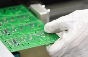
- Component Mounting:
Once the solder paste is applied, the components are mounted on the board. The component placement can be done manually or by using automated machinery. This is a pick and place operation but the components used are required to be confirmed and labeled in the BOM verification stage. The machine or operator picks the labeled component and places it to the designated location.
- Soldering:
Lead-free through-hole or manual soldering is performed in this stage. Regardless of the type of process, THT or SMT, the soldering must be lead-free.
- Board Placement inside Reflow Oven:
The RoHS compatible PCBs are required to be heated at high temperature to evenly melt the solder paste. Therefore, the PCBs are placed inside a reflow oven, where the solder paste melts. Further, the boards are cooled at room temperature to solidify the melted solder paste. This helps fix the components at their position.
- Testing and Packaging:
The PCBs are tested under IPC-600D standards. The solder joints are tested in this step. Visual inspection is followed by AOI and X-ray inspection. Physical and functional testing is performed prior to packaging.
Basic introduction
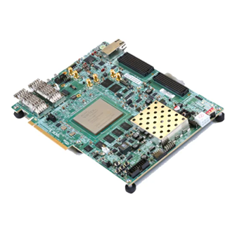
| Name: | 1.6mm HASL Lead Free Circuit Board PCB for household appliances |
| Material | FR/4 all TGs, Aluminum, Ceramic, Teflon, Polyamide, Copper |
| Application | Automotive industry, Power supplies and power converters, Welding equipment |
| Electrical Testing | Fixture / Flying Probe |
| Quality Grade | Ipc Class 2, Ipc Class 3 |
| Silkscreen Colors | Red Oil/Green/Blue/Black/White |
| Other Testing | Aoi, X-ray(Au&Ni), Controlled Impedance Test |
| Placement speed: | Chip component placement speed (at best conditions) 0.036 S/piece |
| Surface Finishes | Immersion Gold, OSP, and HASL |

Our 2 Layer PCB Board Features
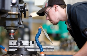
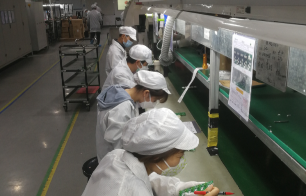
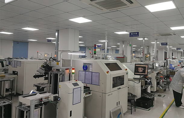
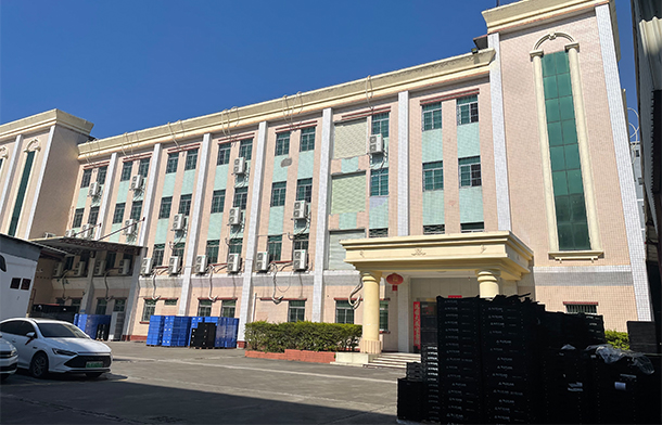
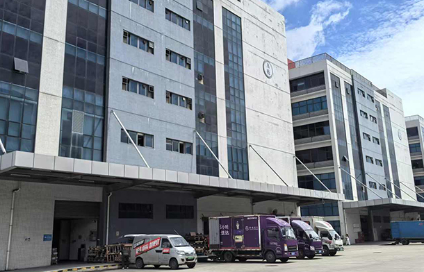
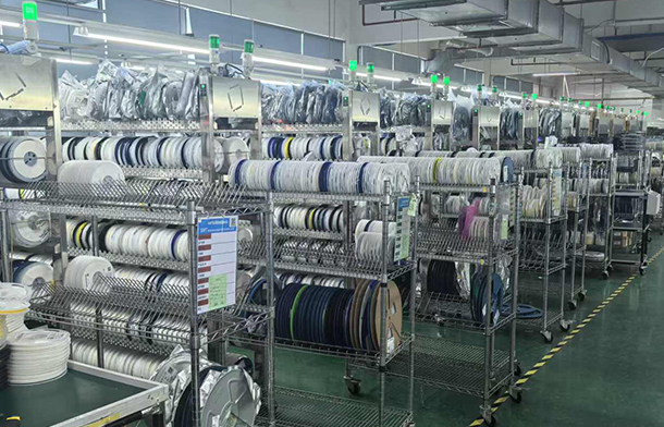
Our PCB Factory Tour
Why choose us for PCB assembly services
Economy
We can provide various types of PCB boards and various materials at competitive prices according to customer requirements.
Best Team
No Matter What Kind Of Pcb Board You Want, Our Trained Designers Can Make lt lnAbout 10-12 Working Days. Emplovees Know The lmportance Of Deadlines, AndTheir Goal ls To Give You Top-Notch Results Within A Specified Time Frame.
Best Team
No Matter What Kind Of Pcb Board You Want, Our Trained Designers Can Make lt lnAbout 10-12 Working Days. Emplovees Know The lmportance Of Deadlines, AndTheir Goal ls To Give You Top-Notch Results Within A Specified Time Frame.
Service
Brnon co0p PchaSn To Functes Candackage Finish , We Provid