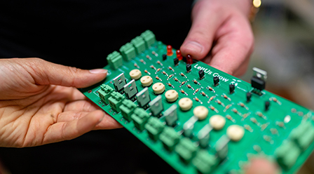
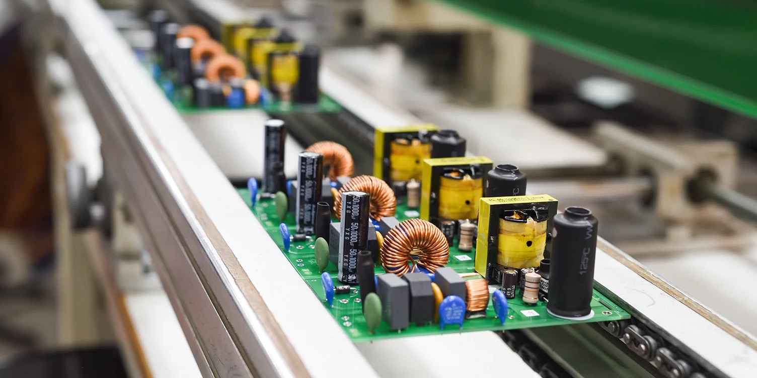
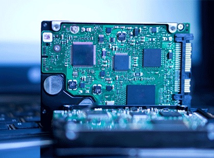
Quality Inspection
We use advanced MES for production line control ,with Fuji NXT,MPM, JUKI, Desen, Suneast and other industry professional equipment, which covers automatic surface mount system , reflow soldering, automatic testing and packaging processes,and production workshop using a fully enclosed air-conditioning system ,temperature and humidity and lighting intensity control ,high standards of electrostatic protection managerment.
98%
99%
-
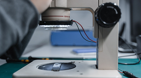
Visual inspection
-
X-ray Inspection
-
3D AOI Testing
-
ICT (In-Circuit Test)
-
FAI
-
AOI Testing
-
3D SPI Testing
-
Functional Test
Visual inspection
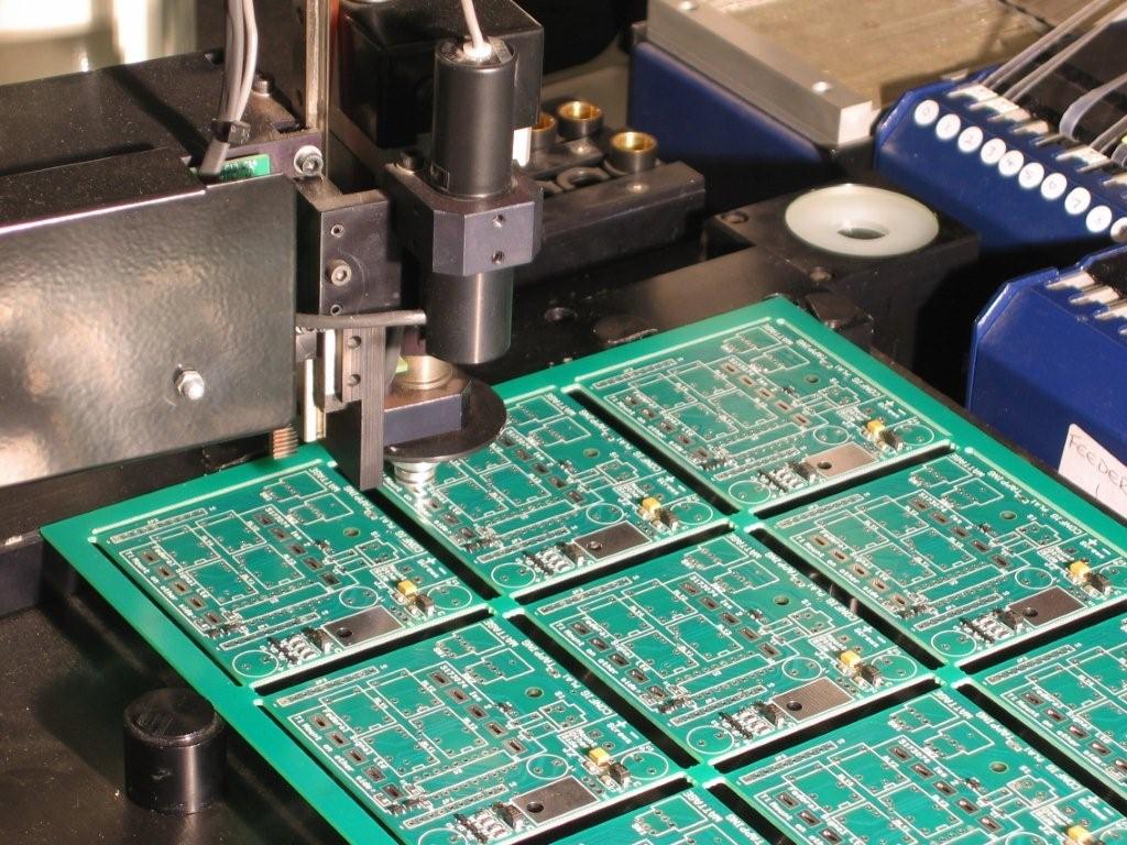
Automated Optical Inspection (AOI) is a tool in circuit board assembly to efficiently and accurately detect production errors before boards leave the facility. AOI uses cameras and image processing software to identify assembly errors such as missing or misplaced components, identifying short circuits, and disconnected components. With more complex boards and larger production quantity this tool improves error detection over visual inspection. AOI machines have seen widespread adoption as surface mount components have miniaturized and board production aims to be more efficient.
Visual inspection is a process in which an individual looks at something with their eyes in order to identify defects, problems, or other issues. It is often used in manufacturing, quality control, and other industries to ensure that products meet certain standards or specifications. Visual inspection can be done by hand or with the aid of visual inspection tools, such as magnifying glasses, microscopes, or cameras. The goal of visual inspection is to detect and correct problems early in the production process, before they become more significant or costly to fix. Visual inspection is typically a quick and inexpensive method of quality control, and it is often used in combination with other inspection methods, such as testing or measurement, to ensure the overall quality of a product.
At Bittele Electronics AOI is one tool we use to provide the best product quality to our turn-key customers. Due to the added labor of setting up the AOI equipment, it is more economical for our clients if we conduct this type of inspection on larger or complex orders as listed in the table below. All of our work is visually inspected by our quality assurance technicians. There is no additional cost when AOI is used, as it is included in our standard assembly services as directed below.
| Order Qty | Component Qty per board | Visual Inspection | AOI |
|---|---|---|---|
| Q<=10< /td> | N/A | Yes | No |
| Q<=10< /td> | N/A | Yes | No |
| Q<=10< /td> | N/A | Yes | No |
| Q<=10< /td> | N/A | Yes | No |
Automated Optical Inspection (AOI)
Automated Optical Inspection (AOI) is a tool in circuit board assembly to efficiently and accurately detect production errors before boards leave the facility. AOI uses cameras and image processing software to identify assembly errors such as missing or misplaced components, identifying short circuits, and disconnected components. With more complex boards and larger production quantity this tool improves error detection over visual inspection. AOI machines have seen widespread adoption as surface mount components have miniaturized and board production aims to be more efficient.
At Bittele Electronics AOI is one tool we use to provide the best product quality to our turn-key customers. Due to the added labor of setting up the AOI equipment, it is more economical for our clients if we conduct this type of inspection on larger or complex orders as listed in the table below. All of our work is visually inspected by our quality assurance technicians. There is no additional cost when AOI is used, as it is included in our standard assembly services as directed below.
X-ray Inspection
PCB (printed circuit board) X-ray inspection is a process in which X-rays are used to examine the internal structure and components of a PCB in order to identify defects or problems. It is often used in manufacturing and quality control to ensure that PCBs meet certain standards or specifications.
During PCB X-ray inspection, the PCB is placed on a stage and X-rays are passed through it. The X-rays are absorbed by different materials in the PCB, such as copper, glass, and plastic, at different levels. This creates a shadow image of the internal structure of the PCB, which can be captured by an X-ray detector and displayed on a computer screen.
PCB X-ray inspection is useful because it allows engineers and technicians to identify defects that may not be visible with the naked eye, such as shorts, opens, and other types of damage to the PCB. It is also useful for examining the internal structure of the PCB, including the placement and orientation of components, to ensure that they are correct.
PCB X-ray inspection is typically used in combination with other inspection methods, such as visual inspection and testing, to ensure the overall quality of the PCB. It is a non-destructive testing method, which means that it does not damage the PCB in any way.
X-ray inspection is a real-time digital imaging system used to detect corrosion under insulation (CUI). Traditionally, to carry out such an inspection, sample areas would have to be identified within the circuit where insulation had to be removed and inspections carried out, which can be time-consuming, costly, and ineffective.
This method utilizes the principle of radiography. The principle of inspection is based on the absorption of gamma radiation in the tested material. A collimated beam of Gadolinium 153 isotopes is used as the source and the photons emitted from the source are received at a receiver. The source and detector are kept external to the pipe and positioned on opposite sides at a fixed distance apart. Gamma rays travel from the source through the pipe to the detector where the photons are received are counted. Proprietary software specially developed for this equipment converts the photon counts and displays a graphical image that corresponds to the pipe’s condition. The scan can reveal density variations caused by corrosion, welds, wet insulation, blockages and any other change in density.
Advantages of x-ray inspection:
- No need for costly insulation removal
- No physical contact is required with the piping and so even high-temperature pipes can be inspected online, meaning no temperature, weather or surface condition limitations.
- No need for surface preparation
- Even non-magnetic, non-metallic pipes can be inspected.
- Can detect wet insulation, which in turn will lead to CUI
- Can detect internal erosion/corrosion and gives absolute values of remaining wall thickness
3D AOI Testing
3D AOI stands for 3D automated optical inspection. 3D AOI inspects assembled printed circuit boards and other electronics in three dimensions. This is in contrast to 2D AOI or two-dimensional automated optical inspection. This typically involves a camera to verify that the items meet quality standards, whether making sure it is the right size or items are in their proper locations.
A 3D AOI system uses vertical and side cameras to see all sides of the board. This is why 3D AOI can recognize when components are skewed or flipped. More intelligent systems can recognize defects like excessive solder joints and uneven solder. These systems rely on multi-stage lighting to provide adequate light for the machine vision lens. Circular lighting is ideally, since it eliminates the possibility of shadows that could cause false calls. One point in favor of 3D AOI is that it can identify defects of 10 ppm or less. This reduces the risk of giving assembled boards a green light when there are actually small defects that should cause it to fail.
- What is PCB 3D AOI testing? PCB 3D AOI testing is a process in which a machine uses cameras and algorithms to automatically inspect PCBs for defects or problems. It is a non-destructive testing method that can be used to identify a wide range of defects, including shorts, opens, missing components, and soldering defects.
- How does PCB 3D AOI testing work? During PCB 3D AOI testing, the PCB is placed on a stage and a camera system captures images of the PCB from multiple angles. These images are then analyzed by algorithms to identify defects or problems. The machine typically uses a combination of 2D and 3D cameras, as well as advanced imaging techniques, to accurately detect defects on the PCB.
- Why is PCB 3D AOI testing used? PCB 3D AOI testing is used to ensure the quality and reliability of PCBs. It allows manufacturers to detect and correct defects early in the production process, before they become more significant or costly to fix. It is also used to reduce the risk of field failures, which can be costly and damaging to a company’s reputation.
- What are the benefits of PCB 3D AOI testing? Some benefits of PCB 3D AOI testing include increased accuracy and speed, reduced inspection costs, and improved product quality. It is a non-destructive testing method, which means that it does not damage the PCB in any way. It is also relatively fast, with some machines able to inspect multiple PCBs per minute.
- Are there any limitations to PCB 3D AOI testing? One potential limitation of PCB 3D AOI testing is that it may not be able to detect all types of defects, especially those that are not visible on the surface of the PCB. It is also limited by the resolution of the cameras and the accuracy of the algorithms used to analyze the images.
ICT (In-Circuit Test)
In circuit test equipment provides a useful and efficient form of printed circuit board test by measuring each component in turn to check that it is in place and of the correct value. As most faults on a board arise out of the manufacturing process and usually consist of short circuits, open circuits or wrong components, this form of testing catches most of the problems on a board. These can easily be checked using simple measurements or resistance, capacitance, and sometimes inductance between two points on the circuit board.
Even when ICs fail, one of the major reasons is static damage, and this normally manifests itself in the areas of the IC close to the connections to the outside world, and these failures can be detected relatively easily using in-circuit test techniques. Some in-circuit tester are able to test some of the functionality of some integrated circuits, and in this way give a high degree of confidence in the build and probability of operation of the board. Naturally an in-circuit test does not give a test of the functionality of a board, but if it has been designed correctly, and then assembled correctly, it should work.
In-circuit test equipment consists of a number of elements:
- In circuit tester: The in circuit test system consists of a matrix of drivers and sensors that are used to set up and perform the measurements. There may be 1000 or more of these driver sensor points. These are normally taken to a large connector conveniently located on the system
- Fixture: The in-circuit test system connector interfaces with the second part of the tester – the fixture. In view of the variety of boards this will be designed specifically for a particular board, and acts as an interface between the board and the in circuit tester. It takes the connections for the driver sensor points and routes them directly to the relevant points on the board using a “bed of nails”.
- Software : Software is written for each board type that can be tested. It instructs the test system what tests to perform, between what points and details of the pass / fail criteria.
These three elements for the major parts of any in-circuit test system. The tester will be used for a variety of boards, while the fixture and software will be board or assembly specific.
In circuit test system are normally relatively expensive items of equipment. They are typically sued on high volume production lines. The fixture and programme generation costs mean that they are not viable for small runs of less than 250 to 1000 items. A cost analysis should be undertaken to ensure that the cost of generating the fixture and programme is viable.
FAI
Femoroacetabular impingement (FAI), also called hip impingement, is a condition where the hip joint is not shaped normally. This causes the bones to painfully rub together. This condition can be treated with corticosteroids, nonsteroidal anti-inflammatory drugs (NSAIDs), physical therapy, rest and surgery.
PCB FAI (First Article Inspection) is a quality control process in which a manufactured printed circuit board (PCB) is inspected to ensure that it meets the design specifications and requirements. It is typically carried out at the beginning of the manufacturing process, before mass production starts.
During the PCB FAI process, a sample of the PCBs is inspected and measured to verify that they meet the required tolerances, dimensions, and other specifications. The process includes visual inspection, measurement of physical characteristics, and functional testing to ensure that the PCBs are of high quality and fit for their intended use.
The PCB FAI process is important because it helps to identify and address any issues or defects in the manufacturing process early on, which can save time and resources by preventing the production of defective PCBs. It is typically carried out by a trained and experienced quality control technician or engineer.
AOI Testing
Automated optical inspection (AOI) technology, also known as machine vision inspection (MVI) technology or automated visual inspection (AVI) technology. In some industries, such as flat panel display, semiconductor, solar, and other manufacturing industries, the term AOI is more popular and known. But AOI and MVI / AVI are still slightly different in concept and function.
In a narrow sense, MVI is an emerging scientific technology that integrates image sensing technology, data processing technology, motion control technology, and performs tasks such as measurement, detection, recognition, and guidance in the industrial production process. The basic principle of MVI uses optical imaging methods (such as a camera, or a complex optical imaging system) to simulate the visual imaging function of the human eye, use a computer processing system instead of the human brain to perform data processing, and finally feedback the results to the implementing agency (such as mechanical Hand) to complete various prescribed tasks instead of manpower.
Broadly speaking, MVI is a technology that stimulates and expands the functions of human eyes, brains, and hands. Its definition may have subtle differences in different application areas, but they cannot leave two fundamental methods and technologies. Obtain the required information from the image, and then feed it back to the automatic actuator to complete the specific task. It can be said that the automatic detection technology based on any image sensing method (such as visible light imaging, infrared imaging, X-ray imaging, ultrasound imaging, etc.) can be considered as MVI or AVI. When using optical imaging methods, MVI actually becomes AOI. Therefore, AOI can be regarded as a special case of MVI.
According to different imaging methods, AOI can be divided into three-dimensional (3D) AOI and two-dimensional (2D) AOI. The three-dimensional AOI is mainly used for the measurement of object shape and geometric parameters, part grouping, positioning, recognition, robot guidance, etc.; AOI is mainly used for product appearance (color, defects, etc.) detection, classification of different objects or appearances, detection, and classification of good and defective products, etc.
3D SPI Testing
3D solder paste inspection, also called SPI is a technique for testing printed circuit boards to make sure that they are printed correctly. You use a machine to monitor the solder paste alignment and volume during the printing process.
3D SPI (Solder Paste Inspection) testing is a process used to inspect and verify the quality of the soldering process in the manufacturing of electronic devices. Solder paste is a material used to join electronic components to a printed circuit board (PCB) during the manufacturing process. 3D SPI testing is a non-destructive inspection method that uses a 3D imaging system to examine the soldering process and identify any defects or issues.
During 3D SPI testing, the soldering process is examined at various stages, including the application of the solder paste, the placement of the electronic components, and the soldering process itself. The 3D imaging system captures high-resolution images of the soldering process, which are then analyzed to identify any defects or issues.
3D SPI testing is an important quality control step in the manufacturing process because it helps to ensure that the soldering process is accurate and reliable. It can help to identify and address any issues early on, which can save time and resources by preventing the production of defective products.
Functional Test
PCB functional testing is a process used to verify that a printed circuit board (PCB) is functioning correctly and meets the required specifications and requirements. It is an important step in the manufacturing process to ensure that the PCBs are of high quality and fit for their intended use.
During the PCB functional test, the PCB is subjected to various tests to ensure that it is functioning properly. These tests may include electrical tests, such as continuity testing and resistance testing, as well as functional tests to ensure that the PCB is able to perform its intended functions.
There are several methods of PCB functional testing, including in-circuit testing (ICT), boundary scan testing, and flying probe testing. These methods use specialized test equipment to verify the functionality of the PCB.
PCB functional testing is an important quality control step in the manufacturing process because it helps to identify and address any issues or defects in the PCBs early on, which can save time and resources by preventing the production of defective products.
Functional testing is a type of testing that seeks to establish whether each application feature works as per the software requirements