

Unlock the Mystery: What Does PCB Stand For in Electronics?
Are you new to electronics and feeling confused about what PCB stands for? Don’t worry, you’ve come to the right place! In this blog, we will answer all your questions about what does PCB stands for in electronics and all you need to know about PCB design.
SECTION 1: Introduction
Printed circuit boards (PCBs) are an essential component of any electronic device. They are used to connect all the components of an electronic device and are the backbone of the device. But what does PCB stand for in electronics?
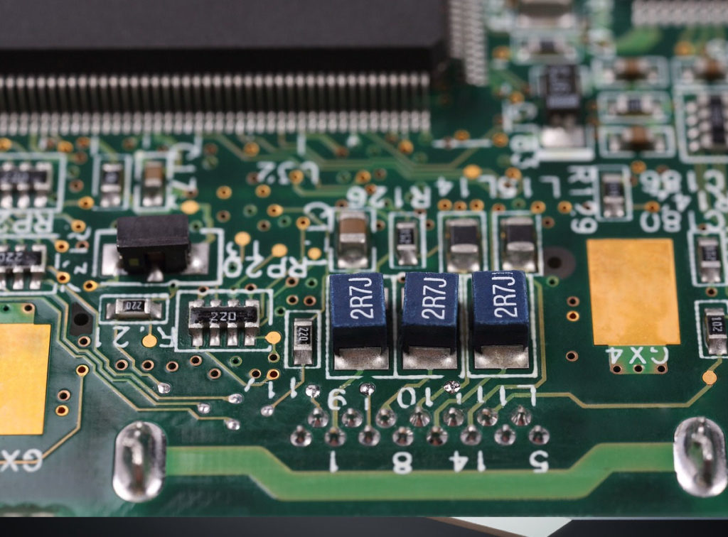
PCB stands for “printed circuit board”. It is an electrical component that is used to control the flow of electricity in a device. It consists of a number of layers of copper-clad laminate material that are etched with the desired electrical circuit pattern.
SECTION 2: What Does PCB Stand For?
As mentioned earlier, PCB stands for “printed circuit board”. It is an electrical component that is used to control the flow of electricity in a device. It consists of a number of layers of copper-clad laminate material that are etched with the desired electrical circuit pattern. The copper layers are used to connect the various components of the device, while the laminate material acts as an insulation layer.
PCBs are used in virtually every electronic device, from phones and computers to home appliances and automobiles. They are used to control the flow of electricity, reduce the risk of short-circuits and make the device more efficient.
SECTION 3: PCB Design Basics
Before you can understand what does PCB stand for in electronics, you need to understand the basics of PCB design. PCB design is the process of creating a PCB that meets your requirements. It involves a series of steps, such as selecting the components, designing the circuit, and testing the prototype.
The design process of a PCB involves the selection of components, designing the circuit, and testing the prototype. The components should be selected based on their functionality, as well as their cost. The circuit should be designed in such a way that it meets the requirements of the device. Once the circuit is designed, it is tested to make sure it works properly.
SECTION 4: Components of a PCB
Now that you know the basics of PCB design, it’s time to look at the components of a PCB. These components are used to connect the various elements of the device and make sure it works properly. The components of a PCB include resistors, capacitors, transistors, integrated circuits, and connectors.
Resistors are used to control the flow of electricity. They are usually made of a metal wire and are used to control the amount of current flowing through the circuit. Capacitors are used to store electrical energy and are used to smooth out fluctuations in the power supply. Transistors are used to amplify signals and are used to switch electrical signals on and off.
Integrated circuits are the heart of the device and are used to process the data. They are made up of multiple components and are used to control the device. Connectors are used to join two or more components together. They are usually made of plastic, metal, or other materials.
SECTION 5: Steps for PCB Design
Once you have selected the components for your PCB, the next step is to design the circuit. This involves creating a schematic diagram of the circuit and laying out the components on the PCB.
The first step is to draw a schematic diagram of the circuit. This step involves drawing a diagram of the circuit that shows all the components and how they are connected. Once the schematic diagram is complete, it is time to lay out the components on the PCB. This involves placing the components on the board in such a way that they are properly connected and do not interfere with each other.
The final step is to test the prototype. This involves testing the circuit to make sure it works properly. Once it is tested and verified to work properly, the PCB is ready to be manufactured.
SECTION 6: PCB Manufacturing Process
Once the PCB is designed and tested, it is ready to be manufactured. The PCB manufacturing process involves a series of steps, such as etching, drilling, plating, and soldering.
The first step is etching. In this step, the copper layers of the PCB are etched with the desired electrical circuit pattern. This is done using a chemical process that removes the unwanted parts of the copper layer.
The next step is drilling. This involves drilling holes into the PCB to allow for the placement of components. The holes are drilled using a CNC machine, which is a computer-controlled machine that can accurately drill holes into the PCB.
The third step is plating. This involves depositing a layer of metal, such as gold or silver, onto the PCB. This is done to prevent oxidation and improve the conductivity of the board.
The last step is soldering. In this step, the components are soldered onto the PCB. This is done using a soldering iron and solder. The soldered connections must be checked to make sure they are secure.
SECTION 7: Benefits of PCB Design
Using PCBs in electronic devices has many benefits. For example, it makes the device more efficient, as it reduces the risk of short-circuits and reduces the number of components that need to be connected. It also makes the device more reliable, as it ensures that all the components are properly connected.
Using PCBs also reduces the cost of manufacturing, as it reduces the number of components that need to be connected. It also makes the device smaller and lighter, as it reduces the size of the components.
Finally, using PCBs in electronic devices makes them easier to repair, as all the components are already connected to the board. This makes it easier for technicians to identify and replace faulty components.
SECTION 8: Common PCB Issues
Despite the many benefits of using PCBs in electronic devices, there are some common issues that can occur. These include shorts, opens, crossovers, and incorrect circuit paths.
Shorts occur when two components are connected incorrectly and the current is flowing between them. Opens occur when a component is not connected properly and the current is not flowing. Crossovers occur when two components are connected incorrectly and the current is flowing between them in the wrong direction.
Incorrect circuit paths occur when the circuit is not designed properly and the components are not connected in the right way. These issues can be avoided by carefully designing the circuit and testing the prototype before manufacturing.
SECTION 9: PCB Design Services
If you don’t have the time or expertise to design your own PCB, you can hire a PCB design service. These services provide expert design services and can help you create a PCB that meets your requirements.
A good PCB design service will have experienced designers who can create a PCB that meets your requirements. They will also be able to provide advice and guidance on the best components to use and the best layout for the circuit.
Finally, a good PCB design service will be able to provide timely delivery of the PCB and ensure that it meets your quality standards.
SECTION 10: Conclusion
In conclusion, PCB stands for “printed circuit board” and is an electrical component used to control the flow of electricity in a device. PCB design is the process of designing a PCB that meets your requirements, and involves the selection of components, designing the circuit, and testing the prototype. The components of a PCB include resistors, capacitors, transistors, integrated circuits, and connectors. The PCB manufacturing process involves etching, drilling, plating, and soldering.
Using PCBs in electronic devices has many benefits, such as improved efficiency, reliability, and cost-effectiveness. However, there are some common issues that can occur, such as shorts, opens, crossovers, and incorrect circuit paths. If you don’t have the time or expertise to design your own PCB, you can hire a PCB design service.
So, now you know what does PCB stand for in electronics and how it is used in electronic devices. We hope that this blog has been helpful and has answered all your questions about PCBs.