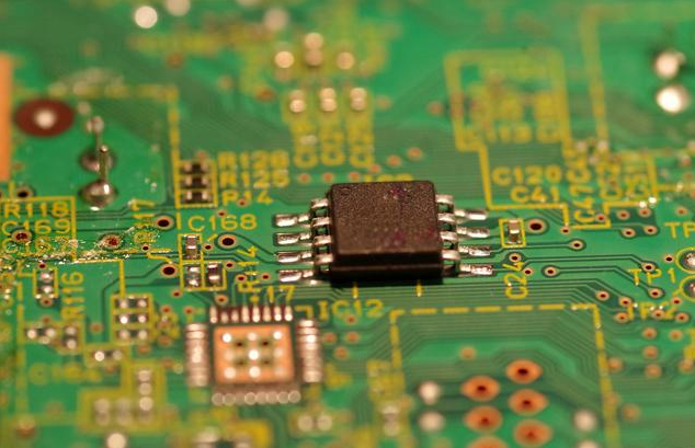
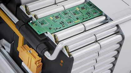
One-Stop Proofing Service: High Frequency PCB
As technology continues to advance, the demand for high frequency PCBs will continue to surge, becoming the backbone of modern electronic systems. WINOW’s one-stop proofing service for high-frequency PCBs offers a seamless experience for clients seeking unparalleled signal integrity and reliability. High Frequency PCB.
When it comes to high-frequency printed circuit boards (PCBs), precision, efficiency, and reliability are paramount. Engineers and designers often face challenges in finding a one-stop solution for their high-frequency PCB needs. However, with WINOW’s comprehensive One-Stop Proofing Service, these challenges can be effortlessly overcome. This blog explores how WINOW’s high-frequency PCB service simplifies the design and manufacturing process, ensuring top-tier performance for diverse applications.
I. The Need for High-Frequency PCBs
The rapid advancement of wireless communication technologies, radar systems, satellite networks, and 5G has spurred the demand for high-frequency PCBs. These specialized boards are designed to handle signals with frequencies exceeding 500 MHz, reaching up to several gigahertz. Their low signal loss, controlled impedance, and reduced electromagnetic interference make them indispensable in critical applications, including aerospace, defense, telecommunications, and medical devices.
II. Understanding WINOW’s One-Stop Proofing Service
2.1 Advanced Design Capabilities
WINOW boasts a team of skilled designers equipped with cutting-edge software and profound expertise in high-frequency PCBs. They collaborate with clients to understand their specific requirements, considering factors like signal integrity, thermal management, and material selection. This collaboration ensures that the final design aligns with the intended application, maximizing performance and minimizing potential issues.
2.2 Material Selection and Trace Routing
Selecting the right material is crucial in high-frequency PCB design. WINOW’s One-Stop Proofing Service offers a wide range of high-quality substrate materials, such as PTFE (Teflon), RF-4, and Rogers RO4000 series, tailored to suit various frequency ranges and environmental conditions. Combined with optimized trace routing, these materials guarantee excellent signal transmission and minimal signal loss.

III. Streamlined Prototyping and Manufacturing
3.1 Rapid Prototyping
WINOW’s One-Stop Proofing Service streamlines the prototyping phase, reducing the time-to-market for high-frequency PCB projects. Through advanced manufacturing capabilities, including 3D printing and laser drilling, the team quickly produces prototype boards for thorough testing and validation, ensuring that the final design meets the client’s requirements.
3.2 Rigorous Quality Control
WINOW’s commitment to quality is evident in its stringent quality control procedures. Each high-frequency PCB undergoes comprehensive testing, including impedance analysis, signal integrity testing, and thermal analysis, to ensure it meets the required specifications. This meticulous approach eliminates the risk of defects and ensures that the PCBs perform flawlessly in demanding applications.
IV. Enhanced Technical Support and Customer Service
4.1 Expert Technical Support
WINOW provides continuous technical support throughout the design, prototyping, and manufacturing processes. Their team of experienced engineers is readily available to address any queries and offer insights to optimize the PCB design further. This level of support is invaluable, particularly for engineers exploring high-frequency PCBs for the first time.
4.2 Tailored Solutions for Diverse Industries
WINOW’s One-Stop Proofing Service caters to a wide array of industries, including aerospace, defense, telecommunications, and medical devices. Whether it’s a complex radar system, a satellite communication module, or a 5G base station, WINOW’s team tailors their high-frequency PCB solutions to match the unique requirements of each industry.
Ⅴ. WINOW – A Leading High-Frequency PCB Manufacturer
With their expertise in high-frequency design, advanced simulation techniques, and global manufacturing capabilities, WINOW proves to be a trusted partner for industries at the forefront of technological innovation. Whether it’s high-speed data transmission or critical signal integrity, WINOW’s high-frequency PCBs provide the foundation for the next generation of cutting-edge electronics.
5.1 Cutting-Edge Technology
WINOW stands at the forefront of the PCB manufacturing industry, equipped with state-of-the-art technology and equipment. Their advanced facilities enable them to produce high-quality HF PCBs with tight tolerances and complex designs.
5.2 Skilled Engineering Team
At WINOW, a team of skilled and knowledgeable engineers is dedicated to delivering top-notch PCB solutions. With years of experience in high-frequency designs, they possess the expertise to tackle even the most intricate challenges effectively.
5.3 Quality Assurance
WINOW takes pride in its commitment to quality. Their stringent quality control measures ensure that each PCB undergoes rigorous testing and inspection, meeting the highest industry standards and customer expectations.
5.4 Customer-Centric Approach
WINOW places a strong emphasis on customer satisfaction. Through effective communication, technical support, and timely delivery, they forge strong partnerships with their clients, providing tailored solutions that cater to individual project requirements.
Ⅵ. Key Considerations in High-Frequency PCB Design
6.1 Impedance Matching: Precision Matters
Impedance matching is crucial in high frequency PCB design to avoid signal reflections and ensure the efficient transfer of signals. WINOW’s team of skilled engineers uses advanced simulation tools to model and optimize impedance throughout the board, ensuring the best possible signal fidelity.
6.2 Material Selection: A Critical Decision
The choice of PCB material significantly influences the performance of high-frequency boards. WINOW offers a diverse range of high-quality materials, such as PTFE and ceramic-filled laminates, with low dielectric loss and excellent electrical properties. These materials enable the precise control of impedance and minimize signal loss, even at high frequencies.
6.3 Layer Stack-Up Design: Balancing Act
In high-frequency PCBs, the layer stack-up design is a delicate balance between maintaining controlled impedance and achieving mechanical stability. WINOW’s engineers are adept at creating stack-up configurations that optimize signal integrity while considering factors like mechanical constraints, heat dissipation, and manufacturing feasibility.
Conclusion
WINOW’s One-Stop Proofing Service for High Frequency PCBs stands as a reliable and efficient solution for engineers and designers seeking top-tier performance in their critical applications. The company’s advanced design capabilities, material selection expertise, streamlined prototyping, and rigorous quality control ensure that clients receive high-frequency PCBs that meet or exceed their expectations. With WINOW as a trusted partner, the journey from concept to reality becomes smooth, empowering industries with cutting-edge technology and seamless communication systems.

