
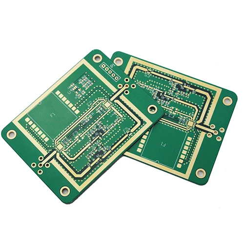
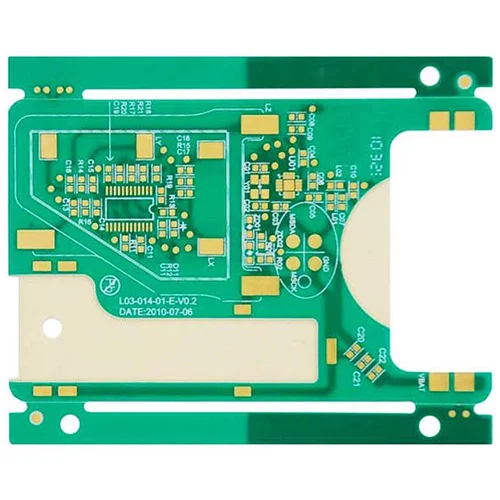
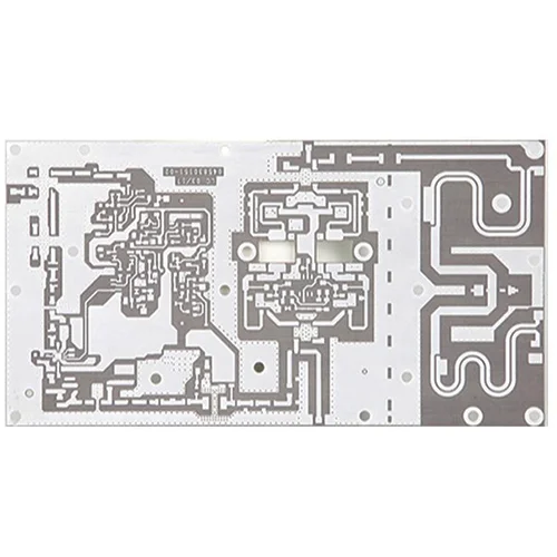
High Frequency PCB Manufacturer
High-frequency printed circuit boards (PCBs) are used in high-frequency electronic devices and systems, typically above 1 GHz. These PCBs are intended to support the transmission of high-frequency signals with as little loss and interference as possible.
Committed to Manufacturing Solutions
What exactly is a High Frequency PCB? A rigid or flex high frequency printed circuit board provides faster signal flow rates and a frequency range of up to 100 GHz. It is important to note that many materials are designed to operate at high frequencies.
We can provide to...
- Turn times as short as 24 hours
- 1 to 100,000 units
- Class II Inspection standard and Class III Inspection available
- 100% on-time guarantee
- DFM support
- Lead free (RoHS) options
- SMT and thru-hole capabilities
- All SMT machine placed
- AOI (Automated Optical Inspection)
- Lead-free RoHS Certification and ITAR compliance screen available
-
Program Design
-
flex Board Capability
-
PCB manufacturing Capabilities
-
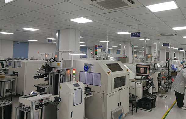
Equipment Exhibition
We offer one-stop services for all types of PCBs, from component purchasing to functional testing and package completion.
Quick payment
Flexible payment options
On-Demand Manufacturing
No MOQ or MPQ limited. Prototype or mass production order acceptable.
Inspection Of Quality
90% of the technical staff have more than 10 years of industry experience
flex Board Capability
| Layer Count | 1-6L 1-4 L normal |
| Board Thickness | 0.1-0.5mm (1-4L) 0.6-0.8mm (5-6L) |
| The tolerance of 1L board thickness | ±0.03mm |
| The tolerance of 2L board thickness | ±0.03mm |
| The tolerance of multilayer board thickness | ±10% (Normal ±0.1mm) |
| The tolerance of multilayer board thickness | ±10% (Normal ±0.05mm) |
| The tolerance of board thickness | ±10% (Normal ±0.1mm) |
| The tolerance of board thickness | 9inch*23inch(PI≥1mil) 9inch*14inch (normal) |
| Max finished board size | 2mm*4mm(no connection tab);8mm*8mm(with connection tab) |
| Min finished board size | 生益 SF305: PI=0.5mil, 1mil, 2mil; Cu=0.33OZ, 0.5OZ, 1OZ |
| Adhesive flex core | 杜邦AP:PI=1mil,2mil,3mil,4mil;Cu=0.5oz,1oz, 2oz |
| Adhesiveless core | 杜邦AP:PI=1mil,2mil,3mil,4mil;Cu=0.5oz,1oz, 2oz |
| Thermosetting adhesive | 杜邦LF:0110,0210 |
| PI stiffener | 台虹 MHK 系列: PI=3mil, 5mil , 7mil, 9mil |
| 3M tape | 9077,9460 |
| Finished copper thickness 12um / 18um | 3/3mil |
| Finished copper thickness 35um | 4/3.5mil |
| Finished copper thickness 70um | 6/5mil |
| Solder mask bridge min. (copper thickness<=1oz) | 4mil(Green),5mil(White),8.0mil(big copper area) |
| Solder mask opening (single side) | 6mil,8mil(big copper area) |
| Solder mask opening of NPTH (single side) | 3mil(partial2.5mil) |
| Min. coverlay bridge | 8mil |
| Finished copper thickness 12um / 18um | 5/5mil (after compensation) |
| Finished copper thickness 35um | 6.5/5mil (after compensation) |
| Finished copper thickness 70um | 10/8mil (after compensation) |
| Min. Inner layer annual ring width | 4mil(<4L),7mil(4-6L),9mil(7-8L) |
| The min distance between inner layer isolated pad and copper area | 3.5mil 4mil normal |
| Max finished inner layer copper thickness | 3oz 2 oz normal |
| Finished copper thickness, before compensation | 3/3mil |
| Finished copper thickness 35um, before compensation | 3.5/3.5mil |
| Finished copper thickness 70um, before compensation | 5.5/5mil |
| Finished copper thickness 35um, | 3mil(<2mm);4mil(2-4.5mm) |
| Finished copper thickness 35-70um, | 5mil(<2mm);6mil(2-4.5mm) |
| Finished copper thickness >70um, | 7mil(<2mm);10mil(2-4.5mm) |
| Min the distance between NPTH edge to external conductor before compensation | 4oz 2 oz normal |
| Max finished external copper thickness | 8mil 5mil(Gold finger area) |
| The max board thickness for 0.15mm drill bit | 0.8mm |
| Min laser hole diameter | 0.1mm |
| Min finish half PTH via diameter | 0.3mm |
| Min NPTH tolerance | ±2mil(limit+0,-2mil or +2mil,-0) |
| Min space between via hole walls in different net, before compensation | 10mil(after compensation) 12mil (normal)(after compensation) |
| Tolerance of stiffener tape | ±0.1mm (Normal ±0.2mm) |
| Tolerance of Coverlay | ±2mil ((Normal ±4mil) |
| Min distance between coverlay opening and conduct | 3mil ((Normal 4mil) |
PCB manufacturing Capabilities
| Normal Tg FR4(Halogen free) | Shengyi S1150 |
| High Tg FR4(Halogen free) | Shengyi S1165 |
| HDI PCB material | LDPP(IT-180A 1037,1086)、Normal 106,1080 |
| High Tg FR4 | Isola:FR408、FR408HR、IS410、FR406、GETEK、PCL-370HR |
| Ceramic Particle Filled Laminates | Rogers:Rogers4350、Rogers4003;Arlon:25FR、25N; |
| PTFE Laminates | Rogers、Taconic、Arlon、Nelco、TP |
| PTFE PP | Taconic:TP、TPN、HT1.5(1.5mil)、Fastrise |
| Rigid PCB | Back board、HDI、 |
| Blind&buried via type | Laminating≤3 times |
| HDI PCB | 1+n+1、1+1+n+1+1、2+n+2、3+n+3 |
| Lead free | Flash gold、ENIG |
| aspect ratio | 10:01:00 |
| Max finished size | HAL Leaded 22"*39" |
| MIN finished size | HAL Leaded 5"*6" |
| PCB thickness | HAL Leaded0.6-4.0mm; |
| MAX high to gold finger | 1.5inch |
| Min space between gold fingers | 6mil |
| Min block space to gold fingers | 7.5mi |
| Max lamination cycle | 3 times |
| Min laser drill for stacked via | 0.1mm |
| Min stacked via pad size | 0.3mm |
| Max laser drilling size | 0.15mm |
| Blind Via Finished Hole Size | 0.3mm |
| Buried Via Finished Hole Size | 0.3mm |
| Non Conductive Filled Vias | 0.2mm~0.8mm |
| Conductive Filled Vias | 0.2~0.8mm |
| ENIG (Electroless Nickel/Immersion Gold) | AU: 0.05~0.1um Nickel: 3~5um |
| Hard gold | 0.1~1.0um |
| Soft gold | 0.1~1.0um |
| Lead Free HASL | 2~40um |
| Flash gold(electroplated gold) | Au 0.025-0.10um,Nickel 3~5um |
| electroplated Gold finger | Au 0.25-1.0um Nickel 3~5um |
| Selective Gold | Au 0.25-1.0um Nickel 3~5um |
| Tin Nickel | N/A |
| Immersion Silver | 0.2~0.4um |
| Soldermask | min. 8um, max. 30um |
| Min mechanical hole 4mil/6mil/8mi | 0.8mm/1.5mm/2.5mm |
| Finshed mechanical hole size | 0.1~6.0mm |
| MAX aspect ratio for Hole | 12:01:00 |
| Max aspect ratio for mechanical depth- control | 1.3:1 |
| Min. depth of Mechanical depth- control(backdrill) | 0.2mm |
| Min gap between hole wall conductor | 7mil |
| Min space between laser holes and conductor | 5mil |
| Min space bwteen hole walls in different net | 12mil |
| Min space bwteen hole walls in same net | 8mil |
| Min space bwteen NPTH hole walls | 10mil |
| Hole location tolerance | '+/-3mil |
| NPTH tolerance | '+/-0.05mm |
| Pressfit holes tolerance | '+/-0.05mm |
| Countersink depth tolerance | '+/-0.15mm |
| Countersink hole size tolerance | '+/-0.15mm |
| Min Pad size for laser drillings | 0.25mm |
| Min Pad size for mechanical drilling | 0.4mm |
| Min Pad size for mechanical drilling | 0.3mm |
| Min BGA pad size | 0.4mm |
| Pad size tolerance(BGA) | '+/-2mil |
| Min lead pitch | 0.3mm |
| Min BGA ball pitch | 0.3mm |
| Internal Layer | 1/3OZ: N/A |
| Internal Layer | 1/2OZ: 3.5/3.5mil |
| Internal Layer | 1OZ: 3/4mil |
| Internal Layer | 2OZ: 4/5mil |
| External Layer | 1/3OZ: 3/3mil |
| External Layer | 1/2OZ:3.5/3.5mil |
| Width tolerance | ≤10mil:+/-20% |
| Min copper pour to Pour | 7mil |
| Min copper pour to trace | 4mil |
| Min copper pour to microvia | 8mil |
| Min copper pour to buired via | 4mil |
| Min copper pour to SMD Pad | 5mil |
| Min copper pour to PTH Pad | 5mil |
| Soldermask color | Semi Gloss greeen\Gloss Green\Matte Green\Black\Red\Blue\Yellow |
| Solder Mask Min Dam Size | 4mil |
| Solder Mask Min Dam Size in BGA Area | 4mil |
| Solder Mask Registration | '+/-4mil |
| Silkscreen color | White, yellow , black |
| Min width of soldermask bridge | White, yellow , black |
| Min width of soldermask bridge | 4mil |
| Min. Diameter Rout Cutter Available | 0.6mm |
| Routed Part Size Tolerance | '+/-0.15mm |
| V-CUT symmetrical tolerance | '+/-0.1mm |
| MAX V-CUT lines | 80 lines |
| V-CUT angle tolerance | '+/-5 degress |
| V Score, Edge to Copper | H≤1.0mm:0.3mm(20°)、0.33mm(30°)、0.37mm(45°); |
| V Score, Edge to Copper | 1.0<H≤1.6mm:0.36mm(20°)、0.4mm(30°)、0.5mm(45°); |
| V Score, Edge to Copper | 1.6<H≤2.4mm:0.42mm(20°)、0.51mm(30°)、0.64mm(45°); |
| V-CUT angle | 20、30、45 degree |
| Gold finger bevelling | 20、30、45、60 degree |
| Gold finger bevelling tolerance | '+/-5 degree |
| Min space of gold finger chamfering | 6mm |
| Min gap between the side of | 8mil |
| Layer count | 1~28 layer |
| PCB thickness | 0.4~6..0mm |
| PCB thickness tolerance˄Normal | Thickness : ±10%(>1.0mm);±0.1mm(≤1.0mm); |
| PCB thickness tolerance˄Special ˅ | Thickness ±0.1mm(≤2.0mm);±0.15mm(2.1-3.0mm) |
| Min bow&twist | 0.75% |
| Controlled Impedance Tolerance | '+/-10% |
| Testing methods | Flying probe testing, Test fixture |
| Quality standards | IPC II, IPC III |


Testing Procedures
High-frequency printed circuit boards (PCBs) are used in a variety of electronic devices, including radio frequency (RF) and microwave devices, and are designed to support high-frequency signals. High-frequency PCBs have the following advantages:
- The PCB material should have a low dielectric loss and a stable dielectric constant. Although FR-4 is a popular material for high-frequency PCBs, other materials such as ceramic-based laminates or low-loss PTFE materials may be used in some cases.
- Trace width and spacing: To minimize signal loss and crosstalk, the width and spacing of the traces on the PCB should be carefully designed.
- Impedance control: The traces’ impedance should be adjusted to match the impedance of the signal source and load. This can be accomplished by using controlled trace width, thickness, and dielectric constant.
- Shielding: Shielding may be required for high-frequency PCBs to reduce the impact of electromagnetic interference (EMI) and to prevent signal loss. This can be accomplished by employing ground planes, copper shielding, and other techniques.
- Layout and routing: The layout and routing of the traces on the PCB should be carefully planned in order to minimize signal loss and crosstalk while maintaining the desired impedance.
- High-frequency PCBs can support a wide range of frequencies and can be designed to operate over a wide temperature range, resulting in improved performance of electronic devices.
- Improved signal integrity: High-frequency PCBs are designed to minimize signal loss and crosstalk, which can result in improved signal integrity and improved electronic device performance.

Bring you better PCB products
Circuit Board Fabrication and PCB Assembly Turnkey Services
High Frequency PCB asked questions
What is a high frequency PCB?
What materials are used to make high frequency PCBs?
How are high frequency PCBs different from regular PCBs?
What are the challenges in designing high frequency PCBs?
How are high frequency PCBs tested?
The assembled PCBs that were delivered worked flawlessly. The component placement is excellent. Mis wang, the WINOW engineer in charge of our project, and I hit it off right away. She asked pertinent questions to ensure that the project was properly completed. We had a very nice, short, and to-the-point conversation.
This board is required to charge my robotic platform's lipo batteries (rover). Excellent communication throughout the ordering process, manufacturing progress, and delivery tracking for a first-time order. Very reasonable price, especially for the first order with a credit for a discount.
The boards arrived yesterday, and assembly has begun. Excellent solder wetting, crisp line definition, and drill holes precisely in the center of via lands.
Please convey my appreciation to everyone who created such fantastic boards.
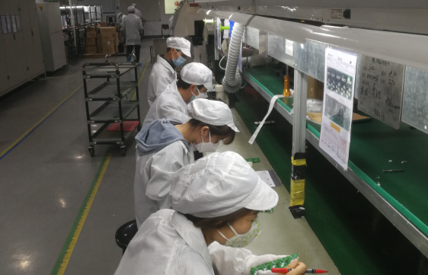
Why Choose Us?
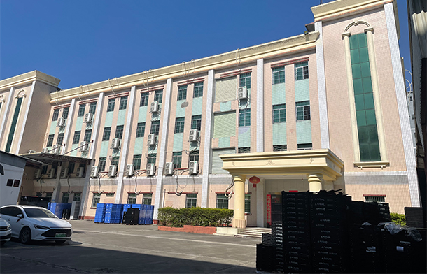
Since 2018, WINOW has been providing high-quality PCBs with quick turnaround times and high customer satisfaction. We are one of the largest and most skilled board manufacturers in China.
-
 Orders for prototypes are processed within 24 hours.
-
PCB prototypes and small-batch manufacturing typically take 5-7 working days.
-
Small batch production and some PCB prototypes have a 48-hour lead time.
Quick payment
Flexible payment options
On-Demand Manufacturing
There is no minimum order or purchase amount. Both prototype and mass production orders are accepted.
Inspection Of Quality
90% of the technical staff has worked in the industry for more than ten years.
Technical Strength
PCB Assembly can be adjusted at any time to meet customer requirements for ICT, veneer, aging, and ATE tests.