

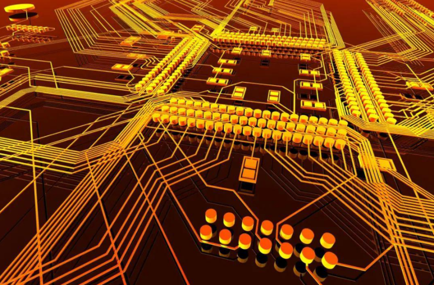
High Speed PCB Design: Critical Requirements & Designs
The electronics manufacturing industry is constantly advancing, and keeping pace requires that manufacturers embrace high speed PCB design. As the demand for faster, more reliable electronic devices continues to rise, the need for high-quality printed circuit boards becomes increasingly important. In this blog, we will take a deep dive into the realm of high-speed PCB design, exploring the requirements and techniques adopted to ensure superior performance. WINOW, a leading producer of first-rate PCBs, has demonstrated proficiency in this area, driving innovation across multiple industries.
I. The Importance of High Speed PCB Design
High Speed PCB design is a crucial discipline that involves careful consideration of signal integrity, electromagnetic interference, and power distribution. With the relentless drive towards miniaturization and higher data transfer rates, designers must push the limits of their PCBs to maintain performance and reliability. As a key enabler of modern technology, high-speed PCB design has opened doors for applications in telecommunications, computing, automotive, aerospace, and more.
As technology continues to advance, WINOW’s commitment to pushing the boundaries of high-speed PCB design will undoubtedly shape the future of modern electronics and open doors to new possibilities. So, the next time you marvel at the speed and precision of your electronic gadgets, remember that it all begins with the remarkable world of high-speed PCB design and the visionary work of manufacturers like WINOW.
II. Critical Requirements for High-Speed PCB Design
1. Signal Integrity (SI)
Signal integrity is paramount in high-speed PCB design. Impedance matching, controlled trace routing, and proper termination are crucial to maintaining signal integrity. Skewed or distorted signals can result in data corruption, leading to system failures. Manufacturers like WINOW invest in advanced simulation and testing tools to validate signal integrity during the design phase, ensuring robust and reliable PCB performance.
2. Controlled Impedance
High-speed PCBs demand precise impedance control to match the characteristic impedance of transmission lines. Maintaining a consistent impedance throughout the board prevents signal reflections, ensuring efficient signal transmission. WINOW utilizes specialized materials and manufacturing techniques to achieve controlled impedance, meeting the stringent requirements of modern high-speed applications.
3. EMI/EMC Considerations
With increasing signal speeds, electromagnetic interference (EMI) and electromagnetic compatibility (EMC) become significant concerns. Shielding, ground planes, and proper component placement are crucial to mitigate EMI/EMC issues. WINOW employs advanced EMI/EMC analysis and design techniques to create PCBs that comply with stringent industry regulations and deliver superior performance in complex electromagnetic environments.
4. High-Frequency Materials
The choice of materials significantly impacts high speed PCB performance. WINOW collaborates with leading material suppliers to source high-quality, low-loss laminates optimized for high-frequency applications. These materials possess excellent dielectric properties, reducing signal attenuation and ensuring reliable data transmission across the board.
5. Differential Pair Routing
High-speed data transmission often involves differential pairs, where two traces carry complementary signals. Properly routing these pairs with controlled spacing and consistent impedance is essential to maintain signal integrity. WINOW’s expert designers leverage differential pair routing techniques to achieve maximum noise immunity and minimize crosstalk between traces.
6. Thermal Management
As data rates increase, high-speed PCBs can generate more heat. Effective thermal management is critical to prevent signal degradation and ensure the longevity of electronic components. WINOW incorporates advanced thermal vias and heat dissipation techniques into their PCB designs, keeping temperatures within optimal ranges.
III. Design Tools and Simulation
1. Utilizing Cutting-Edge Design Software:
High speed PCB design demands sophisticated tools to cope with complex signal analysis and routing challenges. WINOW utilizes advanced PCB design software that integrates signal integrity analysis, 3D visualization, and design rule checks (DRCs). These tools aid in optimizing trace lengths, ensuring signal paths are well-matched, and providing valuable feedback during the design phase.
2. Simulation and Modeling:
Before a high-speed PCB design is brought to life, thorough simulation and modeling are conducted. WINOW employs specialized software to simulate signal propagation, analyze return paths, and predict potential EMI issues. These simulations help validate the design’s performance and guide necessary refinements to achieve optimal results.
IV. Thorough Testing and Validation
1. Prototype Fabrication:
WINOW understands the significance of prototyping in high-speed PCB design. Physical prototypes are crucial for evaluating the design’s functionality, signal integrity, and noise immunity. Prototyping enables designers to identify potential issues early on, reducing costly errors during mass production.
2. Rigorous Testing:
Upon prototype validation, high-speed PCBs undergo rigorous testing to ensure they meet the specified performance criteria. WINOW utilizes advanced testing equipment to verify signal integrity, impedance matching, and overall functionality. Compliance with industry standards and customer requirements is of utmost importance.
Ⅵ. Guidelines for High-Speed PCB Layout and Routing
1. Minimize Signal Traces Length and Cross-Talk
WINOW’s high-speed PCB designs follow the golden rule of minimizing signal trace lengths and keeping them as short as possible. Additionally, they ensure proper spacing between high-speed signal traces to mitigate cross-talk and interference. This meticulous approach eliminates the risk of signal degradation and preserves the integrity of critical data paths.
2. Use of Differential Pairs and Serpentine Routing
Differential pairs play a vital role in high-speed PCBs by reducing electromagnetic interference and enhancing noise immunity. WINOW employs well-matched differential pairs and incorporates serpentine routing to achieve uniform trace lengths, ensuring balanced signal propagation and impedance matching. This methodology enhances signal integrity and reduces the potential for data corruption.
3. Ground Plane Optimization and Decoupling Capacitors
WINOW’s high-speed PCB designs boast optimized ground planes that act as an effective shield against electromagnetic interference (EMI) and ensure a stable reference for signal traces. Furthermore, strategic placement of decoupling capacitors across the PCB helps in reducing power supply noise and enhances overall system stability.
Conclusion:
High Speed PCB Design remains at the forefront of technological advancement, driving innovation and revolutionizing various industries. As electronics continue to permeate every aspect of our lives, manufacturers like WINOW play a crucial role in pushing the boundaries of possibility. By adhering to stringent requirements, utilizing advanced tools, and conducting comprehensive testing, high-speed PCBs continue to empower the world with faster, more efficient, and reliable electronic devices. With WINOW’s commitment to excellence, the future of high-speed PCB design looks promising, and the potential for groundbreaking advancements is limitless.