

PCB Assembly Main LG: What You Need to Know
PCB assembly main LG is a crucial component of the electronics manufacturing process. PCB assembly refers to the process of attaching electronic components to a printed circuit board (PCB) to create a functional electronic device. LG is a leading manufacturer of electronics, and their PCB assembly main LG is an important aspect of their production process.
The PCB assembly main LG process involves a series of steps, including component placement, soldering, inspection, and testing. The process requires a high level of precision and attention to detail to ensure that the electronic device functions properly. LG’s PCB assembly main process is designed to meet the highest standards of quality and reliability, ensuring that their products are of the highest quality.
Overall, the PCB assembly main LG process is an essential aspect of electronics manufacturing. With LG’s commitment to quality and reliability, their PCB assembly main process is sure to produce top-of-the-line electronic devices.
Overview of PCB Assembly
PCB assembly is the process of attaching electronic components to a printed circuit board (PCB). This process is a crucial step in the manufacturing of electronic devices, as it determines the functionality and reliability of the final product. The PCB assembly process involves a series of steps that require precision and attention to detail.
The first step in PCB assembly is the preparation of the board. This involves cleaning the board, applying a solder mask, and adding a silk screen. The solder mask protects the board from excess solder, while the silk screen provides a visual guide for component placement.
The next step is the placement of components. This involves the use of pick-and-place machines, which precisely position components onto the board. The components are then soldered onto the board using either wave soldering or reflow soldering techniques.
After soldering, the board undergoes inspection to ensure that all components are properly placed and soldered. Any defects or issues are identified and corrected at this stage.
Overall, PCB assembly is a complex process that requires expertise and attention to detail. The quality of PCB assembly directly impacts the performance and reliability of electronic devices.
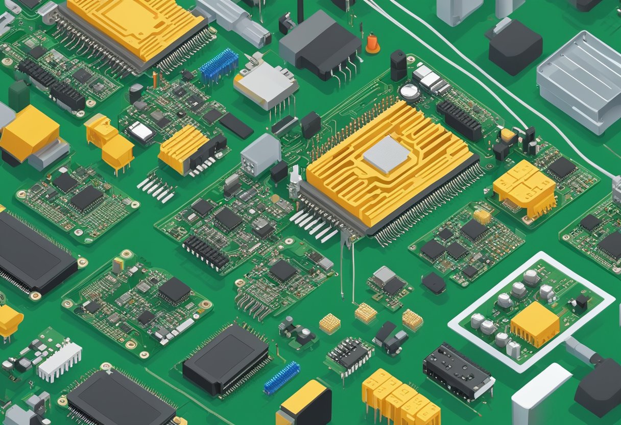
Main Components of LG PCBs
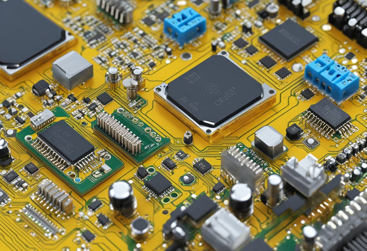
LG PCBs are electronic circuit boards that are used in a wide range of products, from smartphones to televisions. These PCBs are made up of various components that work together to create the desired function. The main components of LG PCBs include capacitors, resistors, and integrated circuits.
Capacitors
Capacitors are electronic components that store energy in an electric field. They are used to filter out noise and to stabilize voltage. Capacitors come in various types, including ceramic, tantalum, and electrolytic. LG PCBs use a combination of these capacitor types to ensure optimal performance.
Resistors
Resistors are electronic components that resist the flow of electric current. They are used to limit current flow, control voltage, and adjust signal levels. LG PCBs use various types of resistors, including carbon film, metal film, and wire wound resistors.
Integrated Circuits
Integrated circuits (ICs) are complex electronic components that contain multiple electronic circuits on a single chip. They are used to perform a wide range of functions, including amplification, signal processing, and data storage. LG PCBs use a variety of ICs, including microcontrollers, memory chips, and power management ICs.
In summary, the main components of LG PCBs include capacitors, resistors, and integrated circuits. These components work together to create the desired function of the PCB. LG uses a combination of these components to ensure optimal performance and reliability.
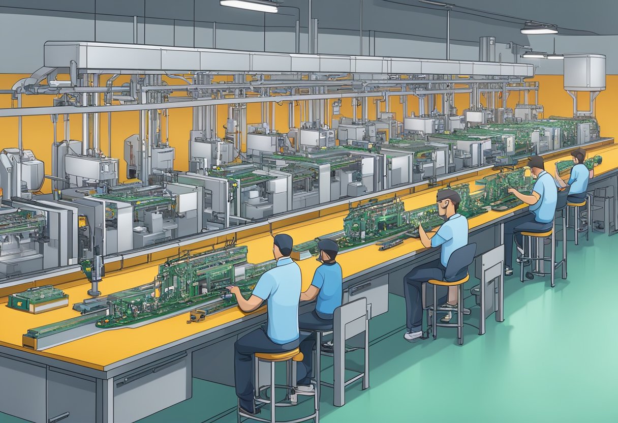
Assembly Process
PCB assembly is a crucial process in the manufacturing of electronic devices. It involves the placement of electronic components onto a printed circuit board (PCB) in order to create a functional electronic device. The assembly process can be broken down into several key steps, including soldering techniques, automated assembly, and quality control.
Soldering Techniques
Soldering is the process of joining two metal surfaces using a filler metal, or solder. There are several soldering techniques used in PCB assembly, including wave soldering, reflow soldering, and hand soldering. Wave soldering involves passing the PCB over a wave of molten solder, which solders the components to the board. Reflow soldering involves heating the PCB and components to a specific temperature, causing the solder to melt and join the components to the board. Hand soldering involves manually applying solder to each individual component.
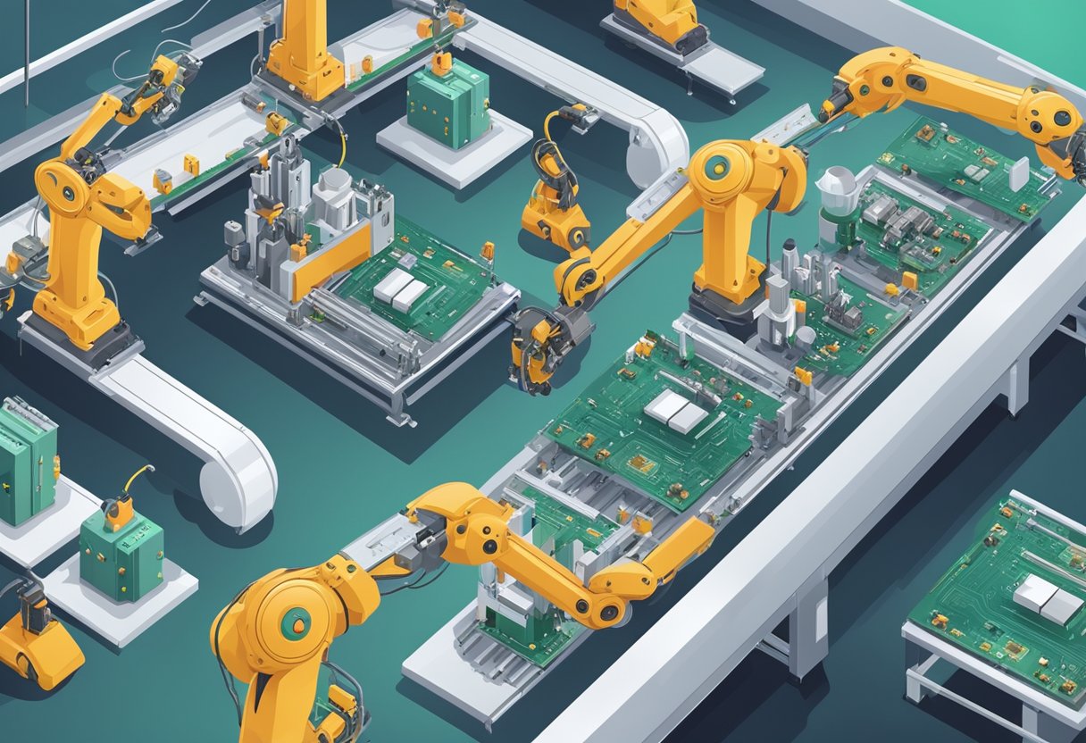
Automated Assembly
Automated assembly is the process of using machines to place and solder components onto a PCB. This process is faster and more efficient than manual assembly, and can be used for both surface-mount and through-hole components. Automated assembly machines use a combination of pick-and-place machines and soldering machines to place and solder components onto the PCB.
Quality Control
Quality control is an essential part of the assembly process. It involves inspecting the PCB and components to ensure that they meet the required standards for functionality and reliability. Quality control checks include visual inspection, automated optical inspection (AOI), and X-ray inspection. AOI uses cameras to inspect the PCB for defects, while X-ray inspection is used to inspect the internal connections of the PCB.
In conclusion, the PCB assembly process is a complex and important process in the manufacturing of electronic devices. By utilizing the appropriate soldering techniques, automated assembly, and quality control measures, manufacturers can ensure that their products are reliable and functional.
Soldering Materials
Lead-Based Solder
Lead-based solder has been the traditional choice for PCB assembly for many years. It is a mixture of tin and lead, typically in a 60:40 ratio. The lead content provides better wetting and flow characteristics, making it easier to work with. However, lead-based solder is now considered hazardous to health and the environment, and its use is being phased out in many countries.
Lead-Free Solder
Lead-free solder is becoming the preferred choice for PCB assembly due to its environmental friendliness. It is a mixture of tin, copper, and silver, with the most common ratio being 96.5% tin, 3% silver, and 0.5% copper. Lead-free solder requires higher temperatures for melting and has a higher surface tension, which can make it more difficult to work with. However, it is a safer and more sustainable option for the long term.
When choosing soldering materials for PCB assembly, it is important to consider the specific requirements of the project, such as the type of components and the desired level of environmental impact. It is also essential to follow proper safety protocols when working with soldering materials to ensure the health and safety of workers and the environment.
Testing and Inspection Methods
When it comes to PCB assembly, testing and inspection are crucial steps to ensure the quality of the final product. There are several methods used for testing and inspection, including visual inspection, automated optical inspection, and functional testing.
Visual Inspection
Visual inspection is the most basic method of testing and inspection. It involves a manual inspection of the PCB assembly to check for any visible defects, such as solder bridges, missing components, or misaligned parts. This method is useful for detecting defects that are visible to the naked eye, but it is not effective for detecting defects that are too small to be seen without magnification.
Automated Optical Inspection
Automated Optical Inspection (AOI) is a more advanced method of testing and inspection. It involves the use of a machine that scans the PCB assembly and compares it to a digital image of the design. The machine can detect defects that are too small to be seen with the naked eye, such as solder shorts, missing components, and misaligned parts. This method is faster and more accurate than visual inspection, but it can be more expensive.
Functional Testing
Functional testing is the most comprehensive method of testing and inspection. It involves testing the PCB assembly to ensure that it functions correctly. This method is useful for detecting defects that may not be visible during visual inspection or AOI, such as incorrect component values or faulty connections. Functional testing can be performed manually or with the use of automated test equipment.
In conclusion, testing and inspection are critical steps in the PCB assembly process. Visual inspection, automated optical inspection, and functional testing are three methods used to ensure the quality of the final product. Each method has its advantages and disadvantages, and the choice of method depends on the specific needs of the project.
PCB Design Considerations
When designing a printed circuit board (PCB), there are several considerations that must be taken into account to ensure proper functionality and reliability. This section will cover some of the most important design considerations for PCB assembly.
Layout and Schematics
The layout and schematics of a PCB are crucial to its functionality. The layout should be designed in a way that minimizes the length of signal traces and reduces the risk of signal interference. The schematics should be clear and easy to read, with all components labeled accurately.
To achieve an optimal layout and schematic design, it is recommended to use PCB design software. These programs allow for easy visualization of the circuit and can help identify potential issues before the board is manufactured.
Thermal Management
Thermal management is another important consideration in PCB design. Components on the board generate heat, and if not properly managed, this heat can lead to component failure and reduced lifespan.
To address thermal management concerns, designers can incorporate heat sinks, thermal vias, and other cooling solutions into the board design. It is also important to ensure proper spacing between components to allow for adequate airflow.
Signal Integrity
Signal integrity is critical to the proper functioning of a PCB. Designers must take steps to minimize noise and interference in the signal path.
To ensure signal integrity, it is important to use appropriate trace widths and spacing, as well as proper grounding techniques. Signal integrity can also be improved through the use of shielding and filtering components.
Overall, careful consideration of these and other design factors can help ensure a reliable and functional PCB assembly.
Surface Mount Technology (SMT)
Surface Mount Technology (SMT) is a method of assembling electronic components onto printed circuit boards (PCBs). In this method, components are mounted directly onto the surface of the PCB, instead of being inserted into holes drilled into the board. SMT has become the preferred method of assembly for most electronic devices due to its many advantages over through-hole technology.
One of the main advantages of SMT is its smaller size. SMT components are generally smaller than through-hole components, which allows for the creation of smaller and more compact devices. This is especially important in applications where space is limited, such as in mobile devices.
Another advantage of SMT is its improved electrical performance. SMT components have shorter leads and a lower profile, which reduces parasitic capacitance and inductance, resulting in better signal integrity. This is particularly important in high-speed digital applications, where signal integrity is critical.
SMT also offers better reliability compared to through-hole technology. Since SMT components are mounted directly onto the surface of the PCB, there is less stress on the component leads, which reduces the risk of mechanical failure. In addition, SMT components are less susceptible to damage from vibration and shock, making them ideal for use in harsh environments.
Overall, SMT has become the preferred method of PCB assembly due to its many advantages over through-hole technology. As electronic devices continue to become smaller and more complex, SMT will continue to play a crucial role in the manufacturing of these devices.
Through-Hole Technology
Through-hole technology (THT) is a method of assembling electronic components onto a printed circuit board (PCB). In this method, the leads of the components are inserted into holes drilled into the PCB and then soldered onto the opposite side of the board.
THT is commonly used for components that require high mechanical strength, such as connectors and power components. It is also preferred for components that need to withstand high temperatures, such as those used in automotive and aerospace applications.
One advantage of THT is that it allows for easy replacement of components, as they can be easily removed and replaced with new ones. This makes it a popular choice for prototyping and small-scale production.
However, THT is not ideal for high-density PCBs, as it takes up more space than surface mount technology (SMT). It also requires more manual labor, which can increase the cost of production.
Overall, THT is a reliable and durable method of PCB assembly that is still widely used in many industries.