

PCB Assembly Process PDF: A Comprehensive Guide
PCB assembly process is a crucial aspect of electronics manufacturing. It involves the assembly of electronic components onto a printed circuit board (PCB) to create a functional electronic device. The process typically involves several stages, including component placement, soldering, inspection, and testing.

To ensure the success of the PCB assembly process, it is important to have a clear understanding of the process flow, the equipment and materials required, and the techniques involved. One valuable resource for this is a PCB assembly process PDF. This document provides a comprehensive overview of the PCB assembly process, including detailed instructions, diagrams, and illustrations to guide the assembly process.
Whether you are a seasoned electronics manufacturer or a beginner looking to learn more about the PCB assembly process, a PCB assembly process PDF can be a valuable resource. By following the guidelines outlined in the document, you can ensure that your PCB assembly process is efficient, effective, and produces high-quality electronic devices.
Overview of PCB Assembly
PCB assembly is a crucial process in the production of electronic devices. It involves the assembly of electronic components onto a printed circuit board (PCB) to create a functional electronic device. This section provides an overview of the PCB assembly process and its various components.
PCB Design and Layout
Before the PCB assembly process can begin, the PCB design and layout must be completed. This involves designing the circuit schematic, creating the PCB layout, and generating the Gerber files. The Gerber files are used to create the PCB, which is then used as the foundation for the assembly process.
Types of PCB Assembly
There are two main types of PCB assembly: through-hole assembly and surface-mount assembly. Through-hole assembly involves inserting components through holes in the PCB and soldering them to the other side of the board. Surface-mount assembly involves soldering components directly onto the surface of the PCB.
Both types of assembly have their advantages and disadvantages. Through-hole assembly is generally more robust and can handle higher power and current levels. Surface-mount assembly, on the other hand, is more compact and can be automated more easily.
In conclusion, PCB assembly is a critical process in the production of electronic devices. The design and layout of the PCB must be completed before the assembly process can begin. There are two main types of PCB assembly, each with its own advantages and disadvantages.
Components Sourcing
When it comes to the PCB assembly process, sourcing components is a crucial step. The quality and availability of components can greatly affect the overall performance and cost of the final product. In this section, we’ll take a closer look at the two main types of components and their form factors.
Active and Passive Components
Active components are those that require a power source to operate, such as transistors, diodes, and integrated circuits. These components are responsible for controlling and amplifying signals within the circuit. Passive components, on the other hand, do not require a power source and include resistors, capacitors, and inductors. These components are used to store and dissipate energy, as well as filter and shape signals.
When sourcing components, it’s important to consider the specifications and tolerances required for each component. For example, resistors and capacitors may need to have specific values and tolerances to ensure proper circuit operation. It’s also important to consider the manufacturer and supplier of the components, as well as their lead times and availability.
Component Form Factors
Component form factors refer to the physical shape and size of the component. This includes through-hole components, surface mount components, and modules. Through-hole components have leads that are inserted into holes on the PCB and soldered on the other side. Surface mount components, on the other hand, are mounted directly onto the surface of the PCB and soldered in place. Modules are pre-assembled components that include multiple active and passive components.
When selecting component form factors, it’s important to consider the space constraints of the PCB, as well as the assembly process. Through-hole components may be easier to solder by hand, while surface mount components require specialized equipment for assembly. Modules can provide a convenient solution for complex circuits, but may have longer lead times and higher costs.
Overall, sourcing components is a critical step in the PCB assembly process. By carefully selecting and evaluating components, manufacturers can ensure the quality and reliability of their final product.
Assembly Process
PCB assembly is a crucial step in the production of electronic devices. It involves several steps that require precision and accuracy to ensure that the final product functions as intended. In this section, we will discuss the various stages involved in the assembly process.
Solder Paste Stenciling
The first step in the assembly process is solder paste stenciling. This involves applying solder paste onto the PCB using a stencil. The stencil is positioned over the PCB, and the solder paste is applied using a squeegee. This process ensures that the solder paste is applied evenly onto the PCB.
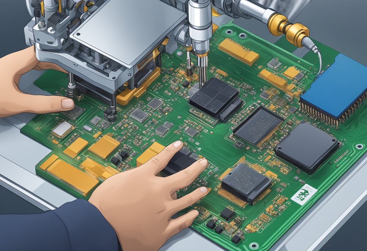
Pick and Place
Once the solder paste has been applied, the next step is pick and place. This involves placing the components onto the PCB. The components are picked up by a machine and placed onto the PCB using a nozzle. This process is automated and ensures that the components are placed accurately onto the PCB.
Reflow Soldering
After the components have been placed onto the PCB, the next step is reflow soldering. This involves heating the PCB to a specific temperature to melt the solder paste and create a permanent bond between the components and the PCB. This process is crucial as it ensures that the components are firmly attached to the PCB.
Manual Assembly and Inspection
In some cases, manual assembly and inspection may be required. This involves manually placing components onto the PCB and inspecting the PCB for any defects. This process is time-consuming and requires a high level of skill and expertise. However, it ensures that any defects are identified and corrected before the final product is assembled.
In conclusion, the PCB assembly process involves several stages that require precision and accuracy to ensure that the final product functions as intended. Each stage is crucial and requires careful attention to detail to ensure that the final product is of high quality.
Testing and Quality Assurance
Automated Optical Inspection
During the PCB assembly process, Automated Optical Inspection (AOI) is a crucial step in ensuring the quality of the finished product. AOI machines use high-resolution cameras and sophisticated software to detect defects such as missing components, incorrect component orientation, and solder joint issues.
One of the benefits of using AOI is that it can quickly and accurately inspect a large number of PCBs, reducing the time and cost associated with manual inspection. Additionally, AOI can detect defects that may not be visible to the human eye, leading to higher quality and reliability of the finished product.
Functional Testing
Functional testing is another important step in the PCB assembly process. This involves testing the PCB to ensure that it meets the required specifications and functions as intended.
Functional testing can be performed manually or through automated testing equipment. Manual testing involves using specialized equipment to test specific components or functions of the PCB. Automated testing, on the other hand, uses software to simulate the operation of the PCB and test its functionality.
Functional testing is critical in ensuring that the PCB meets the required performance standards and is reliable in its intended application. By detecting and addressing any issues early in the testing process, manufacturers can avoid costly recalls and ensure customer satisfaction.
In conclusion, testing and quality assurance are crucial steps in the PCB assembly process. By utilizing AOI and functional testing, manufacturers can ensure the quality and reliability of their finished products, reducing costs and improving customer satisfaction.
Packaging and Delivery
Once the PCB assembly process is complete, the next step is packaging and delivery. This is a crucial step in ensuring that the PCBs are transported safely and securely to their final destination.
Packaging materials used in the PCB assembly process should be sturdy and able to protect the PCBs from any damage during transportation. The packaging materials should also be able to withstand any environmental conditions that the PCBs may be exposed to during shipment.
Before packaging, the PCBs should be inspected to ensure that they meet the required specifications. Any defects or issues should be addressed before packaging to avoid any problems during transportation.
In addition to proper packaging, it is important to choose a reliable and efficient delivery method. The delivery method should be able to provide timely and accurate delivery of the PCBs. It is also important to track the delivery to ensure that the PCBs arrive at their final destination on time.
Overall, proper packaging and delivery are essential in ensuring that the PCB assembly process is successful and that the PCBs are delivered safely and securely to their final destination.