

PCB Design Engineering: Custom Solutins & First Class Service
PCBs are the unsung heroes that power our electronic devices. Whether it’s your smartphone, laptop, or the control panel of your car, PCBs play a crucial role in ensuring these devices function seamlessly. One of the leading manufacturers in the PCB industry, Winow, has been at the forefront of PCB design engineering. In this blog, we will delve into the world of PCB design engineering, exploring its importance, key considerations, and how Winow continues to lead the way in this field.
Winow, a leading manufacturer of PCBs and related services, is renowned for its ability to merge creativity and precision in the design of custom-made PCBs. The company’s dedication to crafting bespoke PCBs tailored to diverse industries and its commitment to quality through rigorous prototyping and testing make it a valuable partner for businesses seeking electronic solutions.
PCB Design Engineering: A Brief View
1. What is PCB Design Engineering?
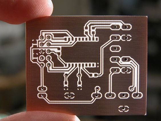
PCB design engineering is the process of creating the layout and schematics for a printed circuit board. It involves meticulously planning the placement of electronic components and designing the intricate pathways (traces) that connect them to form a functional circuit. A well-designed PCB is essential for the reliability and performance of electronic devices.
2. The Importance of PCB Design
A well-designed PCB is the backbone of any electronic device. Here’s why PCB design engineering is crucial:
2.1 Reliability: Reliable PCBs ensure that electronic devices function as intended, without unexpected failures or malfunctions.
2.2 Compactness: Efficient PCB design allows for smaller, more compact devices, which is essential for portable gadgets like smartphones and wearables.
2.3 Optimized Performance: Careful component placement and trace routing can optimize the performance of electronic circuits, minimizing signal interference and maximizing efficiency.
2.4 Cost-Efficiency: Proper PCB design can reduce manufacturing costs by minimizing the use of materials and ensuring efficient assembly processes.
Key Considerations in PCB Design Engineering
1. Component Selection
The selection of components is the foundation of any PCB design. Engineers must choose the right components based on the device’s intended function, performance requirements, and cost considerations. Winow’s expert engineers are well-versed in component sourcing and selection to ensure the best outcomes.
2. Schematic Design
The schematic is a visual representation of the PCB’s electronic connections. It serves as a blueprint for the physical layout. Careful attention to detail during schematic design is essential to avoid costly errors later in the process.
3. Layout and Routing
Efficient layout and routing are critical for signal integrity and performance. Engineers must consider factors like electromagnetic interference (EMI), thermal management, and the physical constraints of the device when designing the PCB layout. Winow’s engineers use advanced software and simulation tools to optimize these aspects.
4. Design for Manufacturability (DFM)
DFM principles are essential to ensure that the PCB design can be manufactured efficiently and cost-effectively. This involves considering factors like penalization, component placement for automated assembly, and adherence to industry standards.
5. Testing and Prototyping
Before mass production, prototypes are crucial to validate the design and identify any potential issues. Winow invests in cutting-edge testing equipment to ensure the highest quality and reliability of their PCBs.
The Design Phase: Where Creativity Meets Precision
1. Crafting the Blueprint
Designing a PCB is akin to creating a detailed blueprint for an intricate electronic circuit. It involves a harmonious blend of creativity and precision. Engineers must meticulously plan the placement of components, ensuring that connections are efficient and compact. Factors like signal integrity, electromagnetic interference (EMI), and thermal management must be considered during this phase. Winow’s experienced team of designers excels in transforming conceptual ideas into functional PCB layouts.
2. Tailoring to Specific Applications
One of the intriguing aspects of PCB design engineering is its adaptability to diverse applications and industries. Whether it’s designing a compact and power-efficient PCB for wearable devices or a rugged, high-performance board for industrial automation, each project comes with its unique challenges. Winow’s expertise lies in tailoring PCB designs to meet the specific requirements of its clients, no matter the industry.
Prototyping: Bringing Concepts to Life
1. From Virtual to Physical
Prototyping is the bridge between theory and reality in the PCB design process. It involves fabricating a physical version of the PCB design to validate its functionality and performance. Winow employs cutting-edge prototyping techniques to bring designs to life, ensuring that they meet the desired specifications. This phase often reveals unforeseen issues that can be addressed before mass production, saving both time and resources.
2. Rigorous Testing
Prototypes undergo rigorous testing, simulating real-world conditions to assess their reliability. This testing phase encompasses functional testing, environmental testing, and EMI/EMC testing to ensure that the PCB can endure the harshest conditions without failure. Winow’s commitment to quality and reliability shines through its exhaustive testing protocols, setting it apart as a trusted manufacturer.
Winow: Leading the Way in PCB Design Engineering
Winow, a renowned manufacturer in the PCB industry, has a proven track record of excellence in PCB design engineering. Their commitment to innovation and quality ensures that their PCBs meet and exceed industry standards. Here’s why Winow stands out:
1. State-of-the-Art Facilities: Winow’s manufacturing facilities are equipped with the latest technology, allowing them to produce high-quality PCBs efficiently.
2. Experienced Engineering Team: Winow boasts a team of experienced engineers who are well-versed in the latest design trends and technologies.
3. Custom Solutions: Winow offers custom PCB design services to meet the unique needs of its clients, whether it’s for consumer electronics, industrial equipment, or automotive applications.
4. Quality Assurance: Winow’s rigorous quality control processes ensure that every PCB they produce meets the highest standards for reliability and performance.
Conclusion
As technology evolves and we push the boundaries of what’s possible, PCB design engineering is at the forefront of innovation. Winow and other industry leaders are poised to shape the future of electronics through their expertise in PCB design and manufacturing. Whether you’re developing the next groundbreaking gadget or a critical component for automotive, understanding the intricacies of PCB design engineering is essential for success in today’s world.