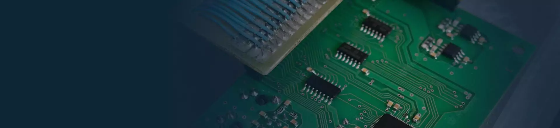
PCB Design
PCB (Printed Circuit Board) design is an essential aspect of modern electronics, and it offers several benefits that make it an attractive option for engineers and designers. Here are some reasons why you might choose PCB design:
PCB Design Manufacturing Solutions
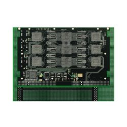
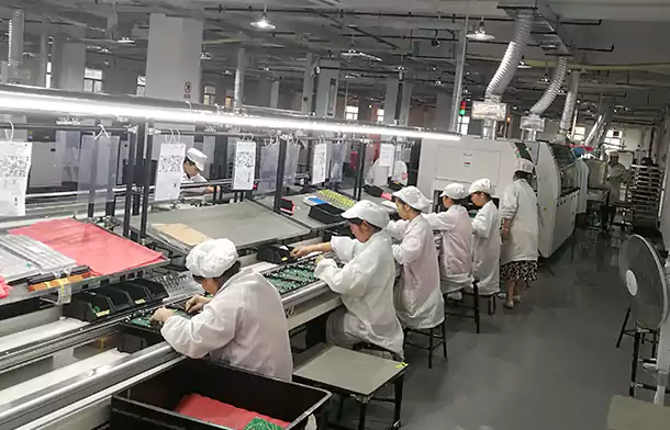
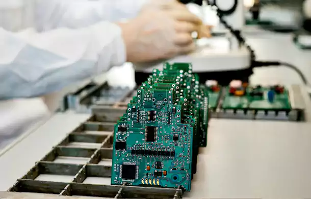
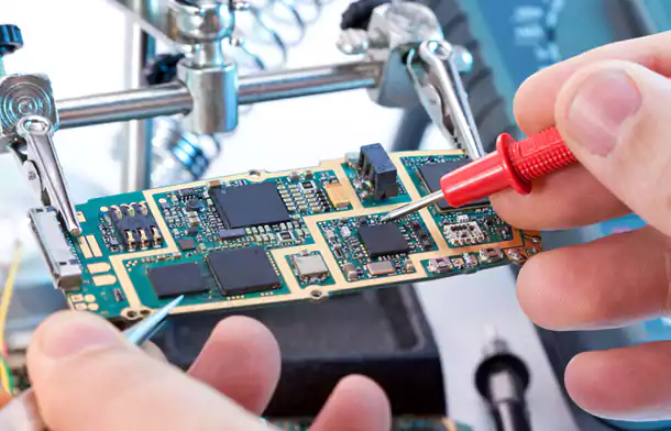
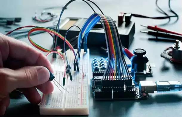
PCB design typically involves the following steps: Schematic capture: This involves creating a diagram of the circuit using specialized software. The diagram shows the various components in the circuit, their connections, and the signals that flow between them. Component selection: Once the schematic is created, the designer selects the components that will be used in the circuit, taking into account factors such as their specifications, availability, and cost. PCB layout: This involves creating a physical layout of the circuit on the PCB substrate. The designer places the components on the board and creates a pattern of electrical traces that connect them. The layout must take into account factors such as signal integrity, power distribution, and heat dissipation. Gerber file generation: Once the layout is complete, the designer generates a set of files called Gerber files that specify the details of the circuit board design, including the placement of components, the routing of traces, and any drill holes or cutouts that are required. PCB fabrication: The Gerber files are sent to a manufacturer, who uses them to fabricate the PCB. This typically involves using a process called photoengraving to create a pattern of conductive traces on the board. Assembly and testing: Once the PCB is fabricated, the components are assembled onto it, typically using automated pick-and-place machines. The completed board is then tested to ensure that it functions correctly.
We can provide to...
- 90% of the technical staff have more than ten years of industry experience, and a PCB design department has been established to provide more professional services.
- To construct PCB packages for the customer (the customer provides the component DATASHEET).
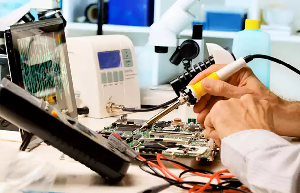
- To provide customers with PCB impedance calculation, lamination design, QA inspection, process inspection, and EMC inspection.
- Supported PCB software formats include Cadence, Mentor ee, Mentor pads, Altium (99SE), and others.
-
Program Design
-
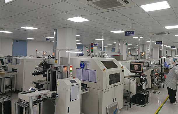
Equipment Exhibition
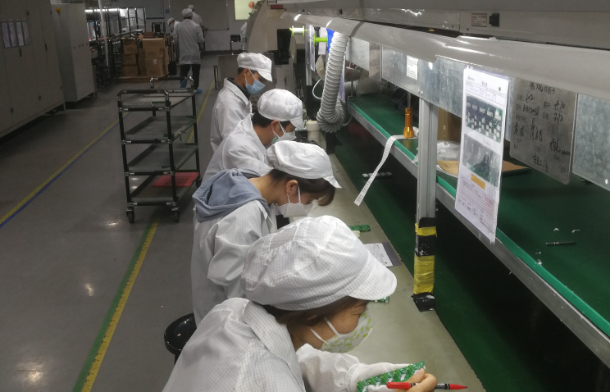
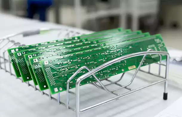
From component purchasing to functional testing and package completion, we provide one-stop services for all types of PCBs.
Quick payment
Flexible payment options
On-Demand Manufacturing
No MOQ or MPQ limited. Prototype or mass production order acceptable.
Inspection Of Quality
90% of the technical staff have more than 10 years of industry experience
Some of the key benefits of DFMA include:
One of the primary benefits of DFMA in construction is the significant reduction of on-site projects due to the use of prefabricated elements.
Reduce assembly costs: DFMA can significantly reduce assembly costs by using fewer parts, requiring less labor, and reducing the number of unique parts.


Bring you better PCB products
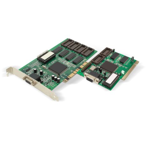
Circuit Board Fabrication and PCB Assembly Turnkey Services
Frequently asked questions
What is a PCB?
What is the purpose of a PCB?
What software is used for PCB design?
What are the key design considerations when creating a PCB?
What is the minimum trace width for a PCB?
What is the minimum clearance between traces on a PCB?
What is a gerber file?
What is a BOM?
What is DFM?
What is DFA?
The delivered assembled PCBs worked flawlessly. The component placement is superb. Mis wang, the WINOW engineer in charge of our project, and I got along great. She asked pertinent questions to ensure that the project was completed properly. We had a very pleasant, quick, and to-the-point conversation.
The assembled PCBs that were delivered worked flawlessly. The component placement is excellent. Mis wang, the WINOW engineer in charge of our project, and I hit it off right away. She asked pertinent questions to ensure that the project was properly completed. We had a very nice, short, and to-the-point conversation.
The boards arrived yesterday and got started on assembly. Excellent solder wetting, clean line definition, and drill holes in the exact center of via lands.
Please convey my appreciation to everyone who created such fantastic boards.
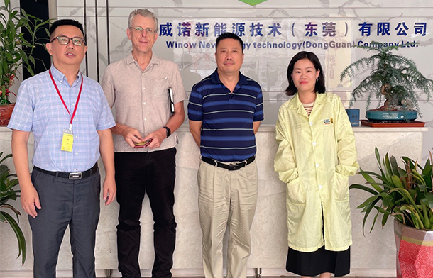
Why Choose Us?
WINOW has been providing high-quality PCBs with fast turnaround times and high customer satisfaction since 2018. We are one of China's largest and most skilled board manufacturers.
-
 Within 24 hours, prototype orders are processed.
-
It usually takes 5-7 working days to complete some PCB prototypes and small-batch manufacturing.
-
A shorter lead time of 48 hours for small batch production and some PCB prototypes.
Quick payment
Flexible payment options
On-Demand Manufacturing
There are no minimum order quantities or minimum purchase quantities. Both prototype and mass production orders are accepted.
Inspection Of Quality
90% of the technical staff has more than ten years of experience in the industry.
Technical Strength
PCB Assembly can be adjusted at any time to meet customer ICT, veneer, aging, and ATE requirements.