Aluminum PCB Manufacturer
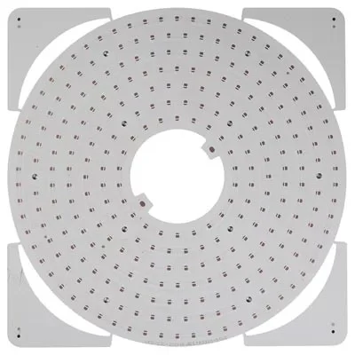
An aluminum PCB, also known as an aluminum-based printed circuit board, is a type of printed circuit board (PCB) that uses aluminum as the base material rather than the standard FR-4 glass fiber-reinforced epoxy resin. Aluminum printed circuit boards (PCBs) are commonly used in applications requiring high thermal conductivity and/or electromagnetic interference (EMI) shielding.
Aluminum PCB Manufacturing Solutions
Aluminum printed circuit boards have a thin layer of conductive dielectric material on them. They are also referred to as Aluminum Clad, Aluminum Base, MCPCB (Metal Clad Printed Circuit Board), IMS (Insulated Metal Substrate), Thermally Conductive PCBs, and other terms. An aluminum PCB's base material is a good heat conductor, making it effective at dissipating heat generated by electronic components. This is especially useful in applications involving high temperatures or high power densities, such as LED lighting and power electronics. Aluminum PCBs can also be used in EMI shielding applications because the aluminum base material effectively blocks the transmission of electromagnetic radiation.
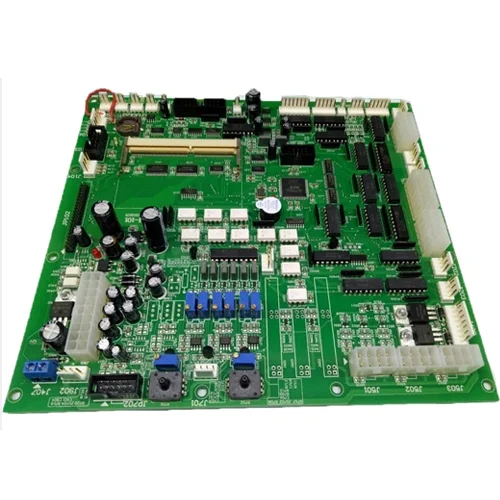
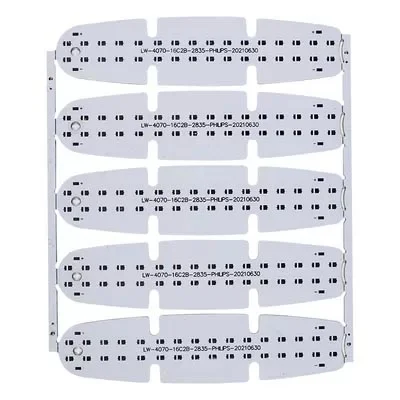
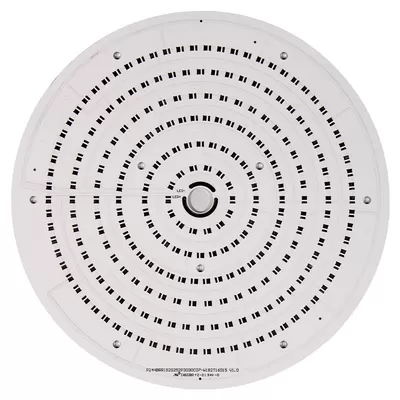
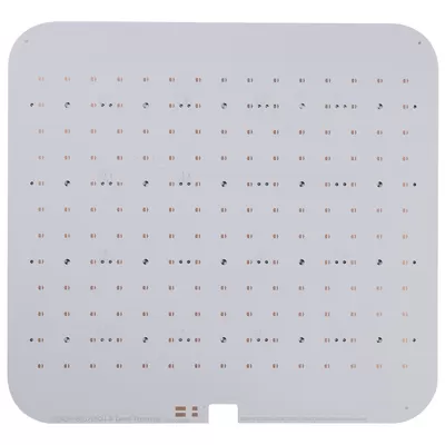
We can provide to...
- Turn times as short as 24 hours
- 1 to 100,000 units
- Class II Inspection standard and Class III Inspection available
- 100% on-time guarantee
- DFM support
- Lead free (RoHS) options
- SMT and thru-hole capabilities
- All SMT machine placed
- AOI (Automated Optical Inspection)
- Lead-free RoHS Certification and ITAR compliance screen available
-
Program Design
-
flex Board Capability
-
PCB manufacturing Capabilities
-
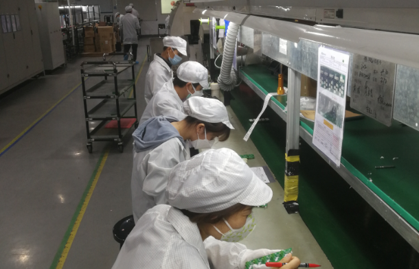
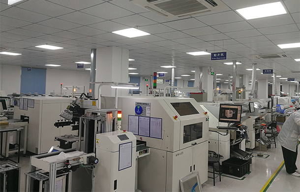
Equipment Exhibition
We offer one-stop services for all types of PCBs, from component purchasing to functional testing and package completion.
flex Board Capability
| Layer Count | 1-6L 1-4 L normal |
| Board Thickness | 0.1-0.5mm (1-4L) 0.6-0.8mm (5-6L) |
| The tolerance of 1L board thickness | ±0.03mm |
| The tolerance of 2L board thickness | ±0.03mm |
| The tolerance of multilayer board thickness | ±10% (Normal ±0.1mm) |
| The tolerance of multilayer board thickness | ±10% (Normal ±0.05mm) |
| The tolerance of board thickness | ±10% (Normal ±0.1mm) |
| The tolerance of board thickness | 9inch*23inch(PI≥1mil) 9inch*14inch (normal) |
| Max finished board size | 2mm*4mm(no connection tab);8mm*8mm(with connection tab) |
| Min finished board size | 生益 SF305: PI=0.5mil, 1mil, 2mil; Cu=0.33OZ, 0.5OZ, 1OZ |
| Adhesive flex core | 杜邦AP:PI=1mil,2mil,3mil,4mil;Cu=0.5oz,1oz, 2oz |
| Adhesiveless core | 杜邦AP:PI=1mil,2mil,3mil,4mil;Cu=0.5oz,1oz, 2oz |
| Thermosetting adhesive | 杜邦LF:0110,0210 |
| PI stiffener | 台虹 MHK 系列: PI=3mil, 5mil , 7mil, 9mil |
| 3M tape | 9077,9460 |
| Finished copper thickness 12um / 18um | 3/3mil |
| Finished copper thickness 35um | 4/3.5mil |
| Finished copper thickness 70um | 6/5mil |
| Solder mask bridge min. (copper thickness<=1oz) | 4mil(Green),5mil(White),8.0mil(big copper area) |
| Solder mask opening (single side) | 6mil,8mil(big copper area) |
| Solder mask opening of NPTH (single side) | 3mil(partial2.5mil) |
| Min. coverlay bridge | 8mil |
| Finished copper thickness 12um / 18um | 5/5mil (after compensation) |
| Finished copper thickness 35um | 6.5/5mil (after compensation) |
| Finished copper thickness 70um | 10/8mil (after compensation) |
| Min. Inner layer annual ring width | 4mil(<4L),7mil(4-6L),9mil(7-8L) |
| The min distance between inner layer isolated pad and copper area | 3.5mil 4mil normal |
| Max finished inner layer copper thickness | 3oz 2 oz normal |
| Finished copper thickness, before compensation | 3/3mil |
| Finished copper thickness 35um, before compensation | 3.5/3.5mil |
| Finished copper thickness 70um, before compensation | 5.5/5mil |
| Finished copper thickness 35um, | 3mil(<2mm);4mil(2-4.5mm) |
| Finished copper thickness 35-70um, | 5mil(<2mm);6mil(2-4.5mm) |
| Finished copper thickness >70um, | 7mil(<2mm);10mil(2-4.5mm) |
| Min the distance between NPTH edge to external conductor before compensation | 4oz 2 oz normal |
| Max finished external copper thickness | 8mil 5mil(Gold finger area) |
| The max board thickness for 0.15mm drill bit | 0.8mm |
| Min laser hole diameter | 0.1mm |
| Min finish half PTH via diameter | 0.3mm |
| Min NPTH tolerance | ±2mil(limit+0,-2mil or +2mil,-0) |
| Min space between via hole walls in different net, before compensation | 10mil(after compensation) 12mil (normal)(after compensation) |
| Tolerance of stiffener tape | ±0.1mm (Normal ±0.2mm) |
| Tolerance of Coverlay | ±2mil ((Normal ±4mil) |
| Min distance between coverlay opening and conduct | 3mil ((Normal 4mil) |
PCB manufacturing Capabilities
| Normal Tg FR4(Halogen free) | Shengyi S1150 |
| High Tg FR4(Halogen free) | Shengyi S1165 |
| HDI PCB material | LDPP(IT-180A 1037,1086)、Normal 106,1080 |
| High Tg FR4 | Isola:FR408、FR408HR、IS410、FR406、GETEK、PCL-370HR |
| Ceramic Particle Filled Laminates | Rogers:Rogers4350、Rogers4003;Arlon:25FR、25N; |
| PTFE Laminates | Rogers、Taconic、Arlon、Nelco、TP |
| PTFE PP | Taconic:TP、TPN、HT1.5(1.5mil)、Fastrise |
| Rigid PCB | Back board、HDI、 |
| Blind&buried via type | Laminating≤3 times |
| HDI PCB | 1+n+1、1+1+n+1+1、2+n+2、3+n+3 |
| Lead free | Flash gold、ENIG |
| aspect ratio | 10:01:00 |
| Max finished size | HAL Leaded 22"*39" |
| MIN finished size | HAL Leaded 5"*6" |
| PCB thickness | HAL Leaded0.6-4.0mm; |
| MAX high to gold finger | 1.5inch |
| Min space between gold fingers | 6mil |
| Min block space to gold fingers | 7.5mi |
| Max lamination cycle | 3 times |
| Min laser drill for stacked via | 0.1mm |
| Min stacked via pad size | 0.3mm |
| Max laser drilling size | 0.15mm |
| Blind Via Finished Hole Size | 0.3mm |
| Buried Via Finished Hole Size | 0.3mm |
| Non Conductive Filled Vias | 0.2mm~0.8mm |
| Conductive Filled Vias | 0.2~0.8mm |
| ENIG (Electroless Nickel/Immersion Gold) | AU: 0.05~0.1um Nickel: 3~5um |
| Hard gold | 0.1~1.0um |
| Soft gold | 0.1~1.0um |
| Lead Free HASL | 2~40um |
| Flash gold(electroplated gold) | Au 0.025-0.10um,Nickel 3~5um |
| electroplated Gold finger | Au 0.25-1.0um Nickel 3~5um |
| Selective Gold | Au 0.25-1.0um Nickel 3~5um |
| Tin Nickel | N/A |
| Immersion Silver | 0.2~0.4um |
| Soldermask | min. 8um, max. 30um |
| Min mechanical hole 4mil/6mil/8mi | 0.8mm/1.5mm/2.5mm |
| Finshed mechanical hole size | 0.1~6.0mm |
| MAX aspect ratio for Hole | 12:01:00 |
| Max aspect ratio for mechanical depth- control | 1.3:1 |
| Min. depth of Mechanical depth- control(backdrill) | 0.2mm |
| Min gap between hole wall conductor | 7mil |
| Min space between laser holes and conductor | 5mil |
| Min space bwteen hole walls in different net | 12mil |
| Min space bwteen hole walls in same net | 8mil |
| Min space bwteen NPTH hole walls | 10mil |
| Hole location tolerance | '+/-3mil |
| NPTH tolerance | '+/-0.05mm |
| Pressfit holes tolerance | '+/-0.05mm |
| Countersink depth tolerance | +/-0.15mm |
| Countersink hole size tolerance | +/-0.15mm |
| Min Pad size for laser drillings | 0.25mm |
| Min Pad size for mechanical drilling | 0.4mm |
| Min Pad size for mechanical drilling | 0.3mm |
| Min BGA pad size | 0.4mm |
| Pad size tolerance(BGA) | '+/-2mil |
| Min lead pitch | 0.3mm |
| Min BGA ball pitch | 0.3mm |
| Internal Layer | 1/3OZ: N/A |
| Internal Layer | 1/2OZ: 3.5/3.5mil |
| Internal Layer | 1OZ: 3/4mil |
| Internal Layer | 2OZ: 4/5mil |
| External Layer | 1/3OZ: 3/3mil |
| External Layer | 1/2OZ:3.5/3.5mil |
| Width tolerance | ≤10mil:+/-20% |
| Min copper pour to Pour | 7mil |
| Min copper pour to trace | 4mil |
| Min copper pour to microvia | 8mil |
| Min copper pour to buired via | 4mil |
| Min copper pour to SMD Pad | 5mil |
| Min copper pour to PTH Pad | 5mil |
| Soldermask color | Semi Gloss greeen\Gloss Green\Matte Green\Black\Red\Blue\Yellow |
| Solder Mask Min Dam Size | 4mil |
| Solder Mask Min Dam Size in BGA Area | 4mil |
| Solder Mask Registration | '+/-4mil |
| Silkscreen color | White, yellow , black |
| Min width of soldermask bridge | White, yellow , black |
| Min width of soldermask bridge | 4mil |
| Min. Diameter Rout Cutter Available | 0.6mm |
| Routed Part Size Tolerance | '+/-0.15mm |
| V-CUT symmetrical tolerance | '+/-0.1mm |
| MAX V-CUT lines | 80 lines |
| V-CUT angle tolerance | '+/-5 degress |
| V Score, Edge to Copper | H≤1.0mm:0.3mm(20°)、0.33mm(30°)、0.37mm(45°); |
| V Score, Edge to Copper | |
| V Score, Edge to Copper | 1.6<H≤2.4mm:0.42mm(20°)、0.51mm(30°)、0.64mm(45°); |
| V-CUT angle | 20、30、45 degree |
| Gold finger bevelling | 20、30、45、60 degree |
| Gold finger bevelling tolerance | '+/-5 degree |
| Min space of gold finger chamfering | 6mm |
| Min gap between the side of | 8mil |
| Layer count | 1~28 layer |
| PCB thickness | 0.4~6..0mm |
| PCB thickness tolerance˄Normal | Thickness : ±10%(>1.0mm);±0.1mm(≤1.0mm); |
| PCB thickness tolerance˄Special ˅ | Thickness ±0.1mm(≤2.0mm);±0.15mm(2.1-3.0mm) |
| Min bow&twist | 0.75% |
| Controlled Impedance Tolerance | '+/-10% |
| Testing methods | Flying probe testing, Test fixture |
| Quality standards | IPC II, IPC III |
PCB Products show
Testing Procedures
Aluminum printed circuit boards (PCBs) have several advantages in electronic devices and systems. Among the primary benefits are:
Aluminum PCBs can effectively dissipate heat, which can improve the performance and lifespan of electronic components. Because they do not warp or delaminate, they are also more durable and have a longer lifespan than traditional PCBs. However, due to the more complex manufacturing process, they are generally more expensive to produce than traditional PCBs.
Aluminum printed circuit boards (PCBs) have several advantages in electronic devices and systems. Among the primary benefits are:
- Thermal management: Because aluminum is a good heat conductor, aluminum printed circuit boards can effectively dissipate heat from electronic components, improving their performance and extending their lifespan.
- Weight savings: Because aluminum is lighter than traditional PCB materials like FR-4, it can help reduce the overall weight of electronic devices and systems.
- Durability: Compared to traditional PCB materials, aluminum PCBs are more resistant to physical damage and environmental factors such as moisture and corrosion. As a result, they are suitable for use in rugged or harsh environments.
- Aluminum PCBs can be more cost-effective than traditional PCB materials in some cases, particularly in high-volume production runs.
- EMI shielding: The use of aluminum PCBs to effectively shield electronic components from EMI, which can improve the reliability and performance of electronic devices and systems.
Aluminum printed circuit boards provide a good combination of performance, durability, and cost-effectiveness, making them a good choice for many electronic applications.
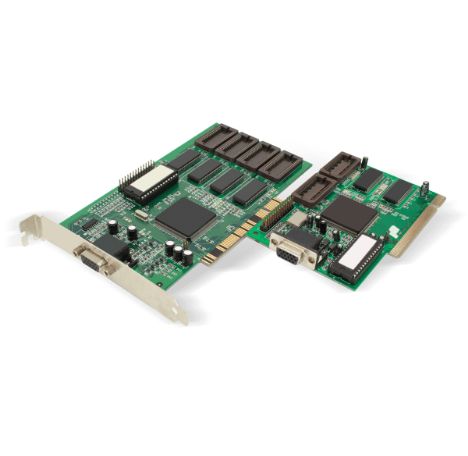

Bring you better PCB products
Circuit Board Fabrication and PCB Assembly Turnkey Services
Aluminum PCB asked questions
What is an aluminum PCB?
What are the advantages of aluminum PCBs?
What are aluminum PCBs used for?
How are aluminum PCBs made?
Can aluminum PCBs be repaired?
Why Choose Us?
WINOW has been providing high-quality PCBs with fast turnaround times and high customer satisfaction since 2018. We are one of China's largest and most skilled board manufacturers.
-
PCB prototypes and small-batch manufacturing typically take 5-7 working days.
-
Orders for prototypes are processed within 24 hours.
-
The lead time for small batch production and some PCB prototypes is 48 hours.
