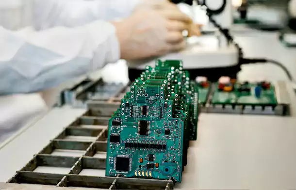
Lead Free PCB Assembly
Lead-free PCB assembly is the process of producing and assembling printed circuit boards (PCBs) with lead-free components and solders. Lead is a toxic metal that has long been used in the production of electronics, but it is now being phased out due to environmental and health concerns.
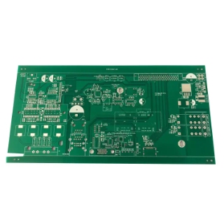
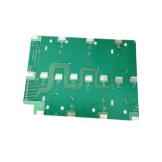
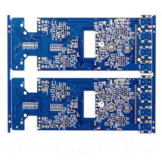
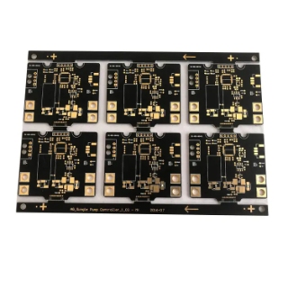
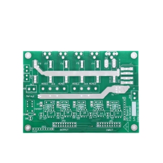
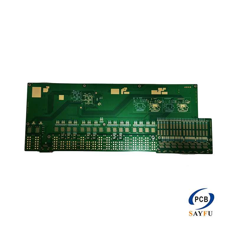
Lead Free PCBs
Rohs PCBs and advanced circuits. As a lead-free solder finish, Advanced Circuits employs a Tin Copper alloy. It's Nihon Superior's SN100CL, a solder that's been around for a while in Asia. It is composed of 99.3% Tin, 0.06% Copper, and some proprietary elements such as nickel.
We can provide to...
- Turn times as short as 24 hours
- 1 to 100,000 units
- Class II Inspection standard and Class III Inspection available
- 100% on-time guarantee
- DFM support
- Lead free (RoHS) options
- SMT and thru-hole capabilities
- All SMT machine placed
- AOI (Automated Optical Inspection)
- Lead-free RoHS Certification and ITAR compliance screen available
-
Program Design
-
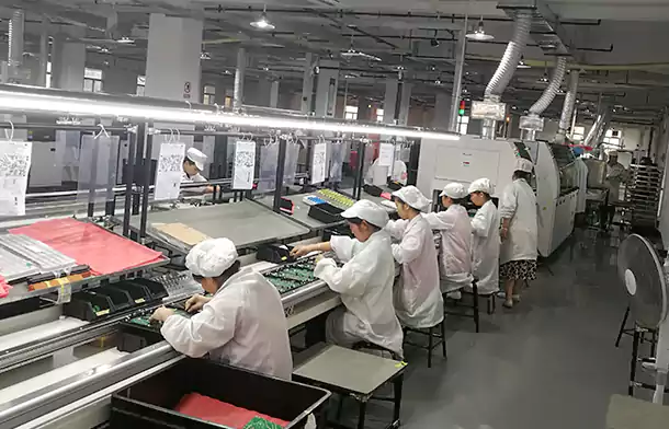
Assembly Capacity
-
SMT Capacity
-
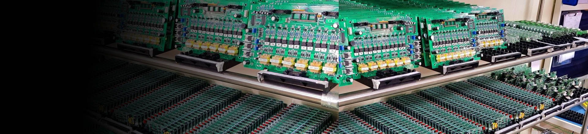
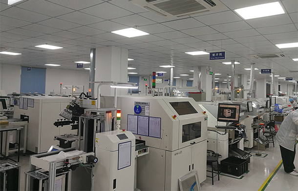
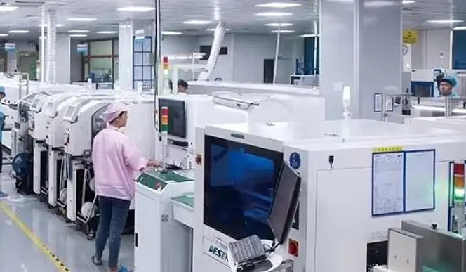
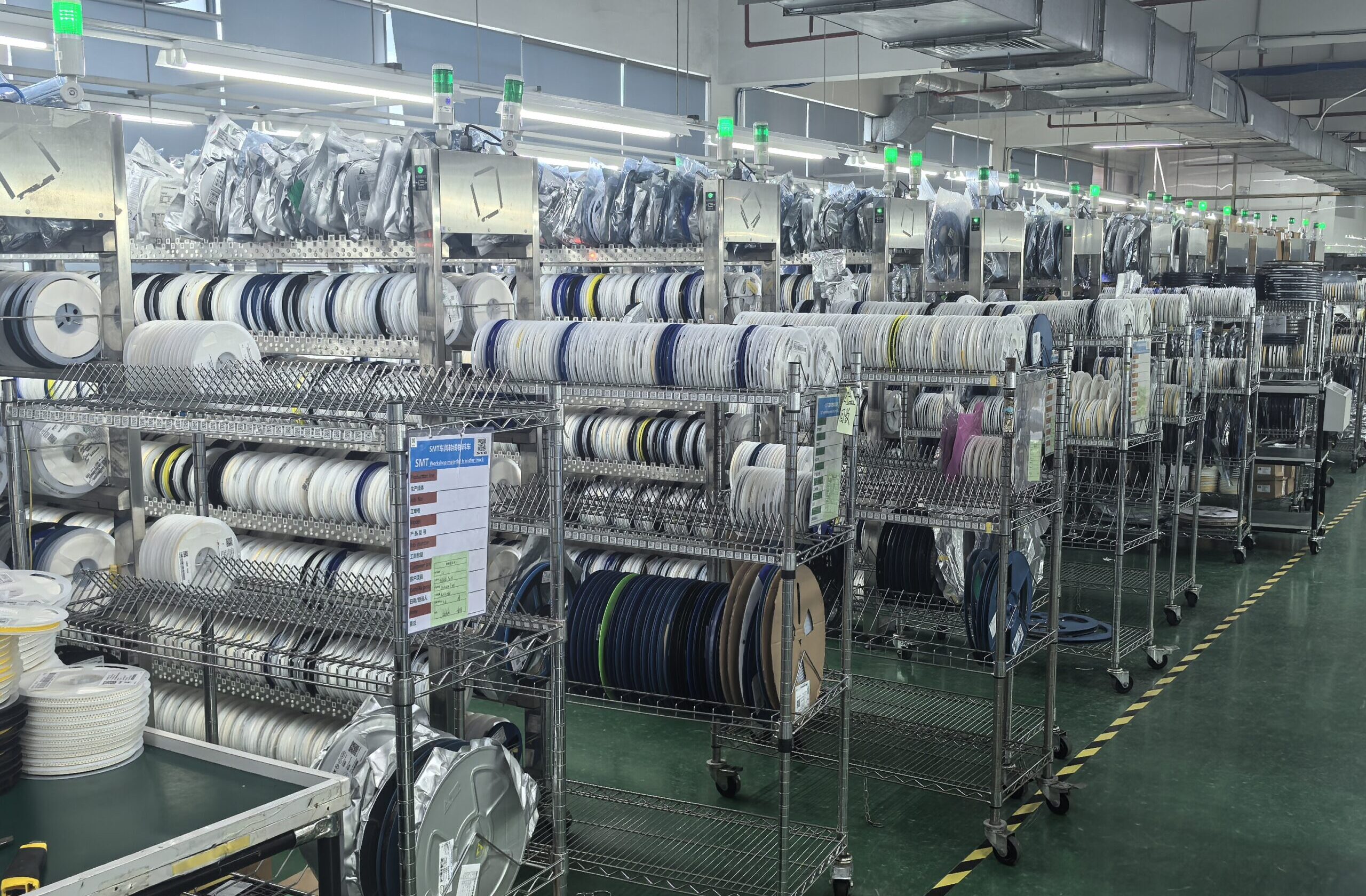
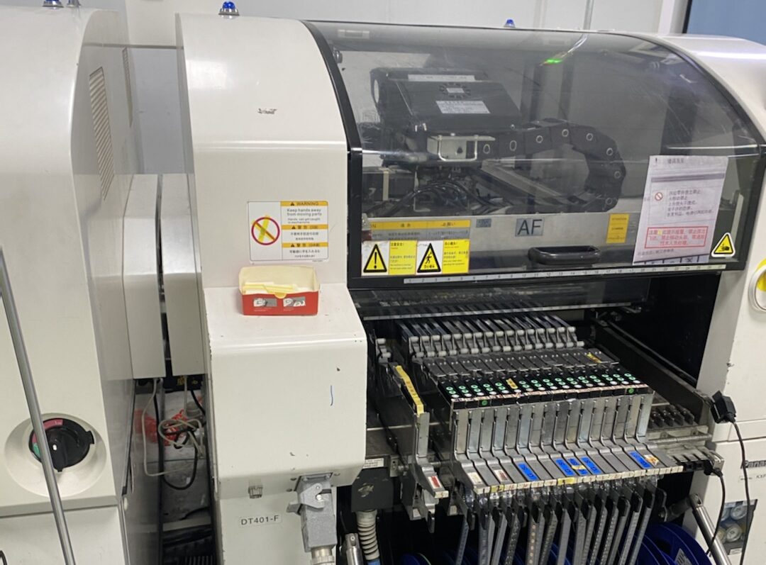
Equipments Exhibition
We offer one-stop services for all types of PCBs, from component procurement to functional testing and package completion.
Quick payment
Flexible payment options
On-Demand Manufacturing
No MOQ or MPQ limited. Prototype or mass production order acceptable.
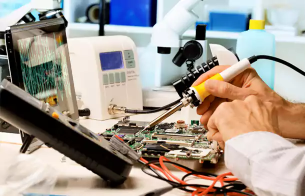
Inspection Of Quality
90% of the technical staff have more than 10 years of industry experience
Assembly Capacity
| Turn-key | Purchase from authorized suppliers, distributors |
| Consigned | Accept parts in reels, cut tapes, tubes & pallets and bulk. |
| Stencils | Offer Laser-cut stainless steel stencil. |
| Solder type | Offer both lead&lead-freeassembly services. |
| Board type | Rigid board, flex board&rigid-flex board. |
| PCB or Panel Size | Min board size of 10*10mm |
| PCB or Panel Size | Max board size of 330*530. |
| Assemble type | The customer provides some components |
| Board shape | There is no limit to shape |
| Prototype | MOQ as low to 5units in 1-2 days delivery |
| Low volume | Offer 3-4 days quick turn time service for low volume. |
| High volumn | Offer accurate delivery to catch your deadline. |
SMT Capacity
| Single and double sided SMT/PTH | Yes |
| Large parts on both sides | Yes |
| BGA on both sides | Yes |
| Smallest Chips size | 201 |
| Min BGA | 0.008 in. (0.2mm) pitch |
| Micro BGA pitch | ball count greater than 1000 |
| Min Leaded parts pitch | 0.008 in. (0.2 mm) |
| Max Parts size | 2.2 in. x 2.2 in. x 0.6 in. |
| Odd form parts: | Yes,Assembly by hands |
| LED | Yes,Assembly by hands |
| Wave soldering | Yes |
| Max PCB size | 14.5 in. x 19.5 in. |
| Min PCB Thickness | 0.02 |
| Fiducial Marks | Preferred but not required |
| PCB Finish: | SMOBC/HASL |
| PCB Finish: | Electrolytic gold |
| PCB Finish: | Electroless gold |
| PCB Finish: | Electroless silver |
| Ball counts | ball count greater than 1000 |
| Resistor | Yes,Assembly by hands |
| Capacitor networks | Yes,Assembly by hands |
| Electrolytic capacitors | Yes,Assembly by hands |
| Variable resistors、capacitors (pots) | Yes,Assembly by hands |
| Sockets | Yes,Assembly by hands |
| PCB Shape | Any |
| Panelized PCB | Tab routed |
| Panelized PCB | Breakaway tabs |
| Panelized PCB | V-Scored |
| Panelized PCB | Routed+ V scored |
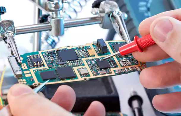
| Inspection | X-ray analysis |
| Inspection | Microscope to 20X |
| Rework | BGA removal and replacement station |
| PCB Finish: | Immersion gold |
| PCB Finish: | Immersion tin |
| PCB Finish: | OSP |


The Electronics Trend: Lead Free PCB Assembly
The process of producing and assembling printed circuit boards (PCBs) with lead-free components and solders is known as lead-free PCB assembly. Lead is a toxic metal that has long been used in electronic manufacturing, but it is being phased out due to environmental and health concerns.
The use of lead-free components and solders is used in lead-free PCB assembly. Alternatives to lead-based solders that can be used in lead-free assembly include tin-silver-copper alloys, tin-copper alloys, and tin-bismuth alloys. Due to their higher melting point than lead-based solders, these alloys can be more difficult to work with and may require specialized equipment and techniques.
As more companies and governments implement regulations to reduce the use of lead in electronics, lead-free PCB assembly is becoming more common. Adopting lead-free assembly can help to protect the environment while also lowering the risk of health problems associated with lead exposure.

Bring you better PCB products
Circuit Board Fabrication and PCB Assembly Turnkey Services
Frequently asked questions
What is lead-free PCB assembly?
Why is lead-free PCB assembly important?
What materials are used in lead-free PCB assembly?
Is lead-free PCB assembly more expensive than traditional PCB assembly?
Are there any regulations governing the use of lead in electronics?
The Printed Circuit Boards were flawlessly assembled. Mis Wang, the WINOW engineer in charge of our project, organized the parts flawlessly. She asked all of the pertinent questions to ensure a successful outcome. We had a very pleasant and productive working relationship with her, and we hope to work with her on future projects again.
This board is required to charge the lipo batteries on my robotic platform (rover). I ordered this item for the first time and was pleased with the excellent communication throughout the ordering process, manufacturing progress, and delivery tracking. It was shipped quickly and arrived on time.
The boards arrived yesterday, and assembly has begun. Outstanding solder wetting, crisp line definition, and drill holes centered on the via lands.
Please convey my gratitude to everyone who created such wonderful boards.
Why Choose Us?
Since 002, Suga Tech has specialized in China's PCB manufacturing and PCB Assembly with over ten years of industry experience. Using your idea or schematic diagram, we can complete the one-stop PCB manufacturing process, which includes design, feasibility analysis, manufacturing, assembly, and testing (Design).
-
 Within 24 hours, prototype orders are processed.
-
It usually takes 5-7 working days to complete some PCB prototypes and small-batch manufacturing.
-
A shorter lead time of 48 hours for small batch production and some PCB prototypes.
Quick payment
Flexible payment options
On-Demand Manufacturing
No MOQ or MPQ limited. Prototype or mass production order acceptable.
Inspection Of Quality
90% of the technical staff has worked in the industry for more than ten years.
Technical Strength
PCB Assembly can be changed at any time to meet the needs of the customer in terms of ICT, veneer, aging, and ATE.