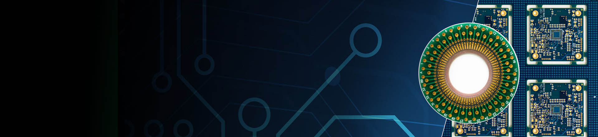
Metal core PCB Manufacturer
A metal core printed circuit board (MCPCB) is a type of printed circuit board (PCB) in which the substrate material is a metal core, typically aluminum or copper, rather than traditional FR-4 fiberglass or CEM-3 composite materials. Metal core PCBs are used in applications where the PCB must efficiently dissipate heat.
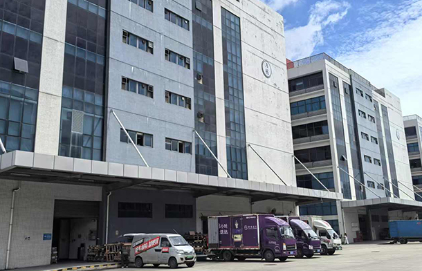
Committed to Manufacturing Solutions
A Metal Core Printed Circuit Board (MCPCB), also known as a thermal PCB or metal-backed PCB, is a type of PCB with a metal material as its base for the heat spreader portion of the board. The thick metal (almost always aluminum or copper) covers one side of the PCB. Many metal-core PCB manufacturers provide a variety of products and services for various applications. When choosing a metal core PCB manufacturer, consider the type of metal core material available, the thickness and thermal conductivity of the metal core, the size and capabilities of the manufacturer's production facilities, and the manufacturer's reputation and track record in the industry.
We can provide to...
- Turn times as short as 24 hours
- 1 to 100,000 units
- Class II Inspection standard and Class III Inspection available
- 100% on-time guarantee
- DFM support
- Lead free (RoHS) options
- SMT and thru-hole capabilities
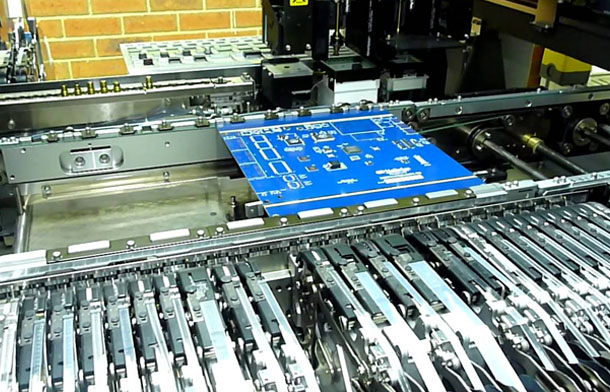
- All SMT machine placed
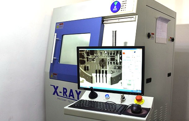
- AOI (Automated Optical Inspection)
- Lead-free RoHS Certification and ITAR compliance screen available
-
Program Design
-
flex Board Capability
-
PCB manufacturing Capabilities
-
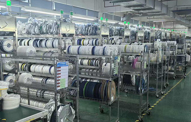
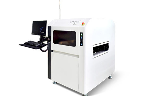
Equipment Exhibition
From component purchasing to functional testing and package completion, we provide one-stop services for all types of PCBs.
Quick payment
Flexible payment options
On-Demand Manufacturing
No MOQ or MPQ limited. Prototype or mass production order acceptable.
Inspection Of Quality
90% of the technical staff have more than 10 years of industry experience
flex Board Capability
| Layer Count | 1-6L 1-4 L normal |
| Board Thickness | 0.1-0.5mm (1-4L) 0.6-0.8mm (5-6L) |
| The tolerance of 1L board thickness | ±0.03mm |
| The tolerance of 2L board thickness | ±0.03mm |
| The tolerance of multilayer board thickness | ±10% (Normal ±0.1mm) |
| The tolerance of multilayer board thickness | ±10% (Normal ±0.05mm) |
| The tolerance of board thickness | ±10% (Normal ±0.1mm) |
| The tolerance of board thickness | 9inch*23inch(PI≥1mil) 9inch*14inch (normal) |
| Max finished board size | 2mm*4mm(no connection tab);8mm*8mm(with connection tab) |
| Min finished board size | 生益 SF305: PI=0.5mil, 1mil, 2mil; Cu=0.33OZ, 0.5OZ, 1OZ |
| Adhesive flex core | 杜邦AP:PI=1mil,2mil,3mil,4mil;Cu=0.5oz,1oz, 2oz |
| Adhesiveless core | 杜邦AP:PI=1mil,2mil,3mil,4mil;Cu=0.5oz,1oz, 2oz |
| Thermosetting adhesive | 杜邦LF:0110,0210 |
| PI stiffener | 台虹 MHK 系列: PI=3mil, 5mil , 7mil, 9mil |
| 3M tape | 9077,9460 |
| Finished copper thickness 12um / 18um | 3/3mil |
| Finished copper thickness 35um | 4/3.5mil |
| Finished copper thickness 70um | 6/5mil |
| Solder mask bridge min. (copper thickness<=1oz) | 4mil(Green),5mil(White),8.0mil(big copper area) |
| Solder mask opening (single side) | 6mil,8mil(big copper area) |
| Solder mask opening of NPTH (single side) | 3mil(partial2.5mil) |
| Min. coverlay bridge | 8mil |
| Finished copper thickness 12um / 18um | 5/5mil (after compensation) |
| Finished copper thickness 35um | 6.5/5mil (after compensation) |
| Finished copper thickness 70um | 10/8mil (after compensation) |
| Min. Inner layer annual ring width | 4mil(<4L),7mil(4-6L),9mil(7-8L) |
| The min distance between inner layer isolated pad and copper area | 3.5mil 4mil normal |
| Max finished inner layer copper thickness | 3oz 2 oz normal |
| Finished copper thickness, before compensation | 3/3mil |
| Finished copper thickness 35um, before compensation | 3.5/3.5mil |
| Finished copper thickness 70um, before compensation | 5.5/5mil |
| Finished copper thickness 35um, | 3mil(<2mm);4mil(2-4.5mm) |
| Finished copper thickness 35-70um, | 5mil(<2mm);6mil(2-4.5mm) |
| Finished copper thickness >70um, | 7mil(<2mm);10mil(2-4.5mm) |
| Min the distance between NPTH edge to external conductor before compensation | 4oz 2 oz normal |
| Max finished external copper thickness | 8mil 5mil(Gold finger area) |
| The max board thickness for 0.15mm drill bit | 0.8mm |
| Min laser hole diameter | 0.1mm |
| Min finish half PTH via diameter | 0.3mm |
| Min NPTH tolerance | ±2mil(limit+0,-2mil or +2mil,-0) |
| Min space between via hole walls in different net, before compensation | 10mil(after compensation) 12mil (normal)(after compensation) |
| Tolerance of stiffener tape | ±0.1mm (Normal ±0.2mm) |
| Tolerance of Coverlay | ±2mil ((Normal ±4mil) |
| Min distance between coverlay opening and conduct | 3mil ((Normal 4mil) |
PCB manufacturing Capabilities
| Normal Tg FR4(Halogen free) | Shengyi S1150 |
| High Tg FR4(Halogen free) | Shengyi S1165 |
| HDI PCB material | LDPP(IT-180A 1037,1086)、Normal 106,1080 |
| High Tg FR4 | Isola:FR408、FR408HR、IS410、FR406、GETEK、PCL-370HR |
| Ceramic Particle Filled Laminates | Rogers:Rogers4350、Rogers4003;Arlon:25FR、25N; |
| PTFE Laminates | Rogers、Taconic、Arlon、Nelco、TP |
| PTFE PP | Taconic:TP、TPN、HT1.5(1.5mil)、Fastrise |
| Rigid PCB | Back board、HDI、 |
| Blind&buried via type | Laminating≤3 times |
| HDI PCB | 1+n+1、1+1+n+1+1、2+n+2、3+n+3 |
| Lead free | Flash gold、ENIG |
| aspect ratio | 10:01:00 |
| Max finished size | HAL Leaded 22"*39" |
| MIN finished size | HAL Leaded 5"*6" |
| PCB thickness | HAL Leaded0.6-4.0mm; |
| MAX high to gold finger | 1.5inch |
| Min space between gold fingers | 6mil |
| Min block space to gold fingers | 7.5mi |
| Max lamination cycle | 3 times |
| Min laser drill for stacked via | 0.1mm |
| Min stacked via pad size | 0.3mm |
| Max laser drilling size | 0.15mm |
| Blind Via Finished Hole Size | 0.3mm |
| Buried Via Finished Hole Size | 0.3mm |
| Non Conductive Filled Vias | 0.2mm~0.8mm |
| Conductive Filled Vias | 0.2~0.8mm |
| ENIG (Electroless Nickel/Immersion Gold) | AU: 0.05~0.1um Nickel: 3~5um |
| Hard gold | 0.1~1.0um |
| Soft gold | 0.1~1.0um |
| Lead Free HASL | 2~40um |
| Flash gold(electroplated gold) | Au 0.025-0.10um,Nickel 3~5um |
| electroplated Gold finger | Au 0.25-1.0um Nickel 3~5um |
| Selective Gold | Au 0.25-1.0um Nickel 3~5um |
| Tin Nickel | N/A |
| Immersion Silver | 0.2~0.4um |
| Soldermask | min. 8um, max. 30um |
| Min mechanical hole 4mil/6mil/8mi | 0.8mm/1.5mm/2.5mm |
| Finshed mechanical hole size | 0.1~6.0mm |
| MAX aspect ratio for Hole | 12:01:00 |
| Max aspect ratio for mechanical depth- control | 1.3:1 |
| Min. depth of Mechanical depth- control(backdrill) | 0.2mm |
| Min gap between hole wall conductor | 7mil |
| Min space between laser holes and conductor | 5mil |
| Min space bwteen hole walls in different net | 12mil |
| Min space bwteen hole walls in same net | 8mil |
| Min space bwteen NPTH hole walls | 10mil |
| Hole location tolerance | '+/-3mil |
| NPTH tolerance | '+/-0.05mm |
| Pressfit holes tolerance | '+/-0.05mm |
| Countersink depth tolerance | '+/-0.15mm |
| Countersink hole size tolerance | '+/-0.15mm |
| Min Pad size for laser drillings | 0.25mm |
| Min Pad size for mechanical drilling | 0.4mm |
| Min Pad size for mechanical drilling | 0.3mm |
| Min BGA pad size | 0.4mm |
| Pad size tolerance(BGA) | '+/-2mil |
| Min lead pitch | 0.3mm |
| Min BGA ball pitch | 0.3mm |
| Internal Layer | 1/3OZ: N/A |
| Internal Layer | 1/2OZ: 3.5/3.5mil |
| Internal Layer | 1OZ: 3/4mil |
| Internal Layer | 2OZ: 4/5mil |
| External Layer | 1/3OZ: 3/3mil |
| External Layer | 1/2OZ:3.5/3.5mil |
| Width tolerance | ≤10mil:+/-20% |
| Min copper pour to Pour | 7mil |
| Min copper pour to trace | 4mil |
| Min copper pour to microvia | 8mil |
| Min copper pour to buired via | 4mil |
| Min copper pour to SMD Pad | 5mil |
| Min copper pour to PTH Pad | 5mil |
| Soldermask color | Semi Gloss greeen\Gloss Green\Matte Green\Black\Red\Blue\Yellow |
| Solder Mask Min Dam Size | 4mil |
| Solder Mask Min Dam Size in BGA Area | 4mil |
| Solder Mask Registration | '+/-4mil |
| Silkscreen color | White, yellow , black |
| Min width of soldermask bridge | White, yellow , black |
| Min width of soldermask bridge | 4mil |
| Min. Diameter Rout Cutter Available | 0.6mm |
| Routed Part Size Tolerance | '+/-0.15mm |
| V-CUT symmetrical tolerance | '+/-0.1mm |
| MAX V-CUT lines | 80 lines |
| V-CUT angle tolerance | '+/-5 degress |
| V Score, Edge to Copper | H≤1.0mm:0.3mm(20°)、0.33mm(30°)、0.37mm(45°); |
| V Score, Edge to Copper | 1.0<H≤1.6mm:0.36mm(20°)、0.4mm(30°)、0.5mm(45°); |
| V Score, Edge to Copper | 1.6<H≤2.4mm:0.42mm(20°)、0.51mm(30°)、0.64mm(45°); |
| V-CUT angle | 20、30、45 degree |
| Gold finger bevelling | 20、30、45、60 degree |
| Gold finger bevelling tolerance | '+/-5 degree |
| Min space of gold finger chamfering | 6mm |
| Min gap between the side of | 8mil |
| Layer count | 1~28 layer |
| PCB thickness | 0.4~6..0mm |
| PCB thickness tolerance˄Normal | Thickness : ±10%(>1.0mm);±0.1mm(≤1.0mm); |
| PCB thickness tolerance˄Special ˅ | Thickness ±0.1mm(≤2.0mm);±0.15mm(2.1-3.0mm) |
| Min bow&twist | 0.75% |
| Controlled Impedance Tolerance | '+/-10% |
| Testing methods | Flying probe testing, Test fixture |
| Quality standards | IPC II, IPC III |

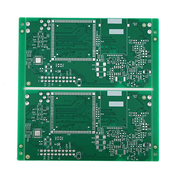
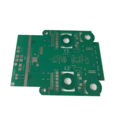
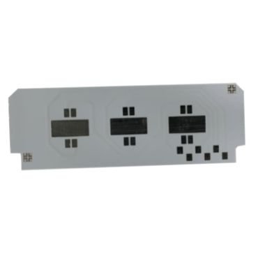
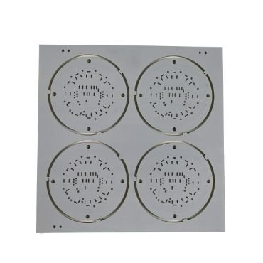
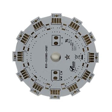
PCB Products show
Metal Core PCB Manufacturers and Benefits Overview
To find a metal core PCB manufacturer, you can start by searching online and looking for companies that specialize in the type of metal core PCBs you need. You can also ask for recommendations from industry professionals or other PCB users. It may also be helpful to visit trade shows and conferences, where you can meet and talk with different manufacturers and see their products in person.
There are several advantages to using metal core PCBs over traditional printed circuit boards:
- Heat dissipation: A metal core PCB acts as a heatsink, allowing it to dissipate heat more effectively than a traditional PCB. This is especially useful in applications where the PCB must dissipate a significant amount of heat, such as power electronics and LED lighting.
- Thermal stability: The metal core has a more stable and consistent thermal expansion coefficient, which can help prevent warping or cracking due to temperature changes.
- Improved performance: Metal core PCBs’ improved heat dissipation and thermal stability can lead to improved performance and reliability in high-power and high-temperature applications.
- Reduced component stress: The metal core can help distribute heat evenly across the PCB, reducing stress and extending component life.
- Metal core PCBs can be customized with various metal core materials, thicknesses, and shapes to meet the specific needs of various applications.
- Cost-effectiveness: While metal core PCBs are more expensive up front, their improved performance and lifespan can make them more cost-effective in the long run, especially in applications where traditional PCBs would fail due to heat or other environmental conditions.

Bring you better PCB products
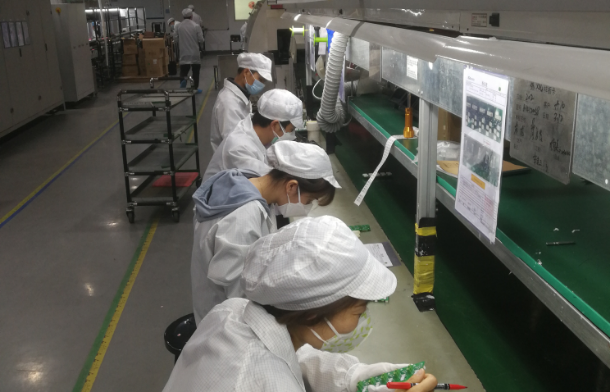
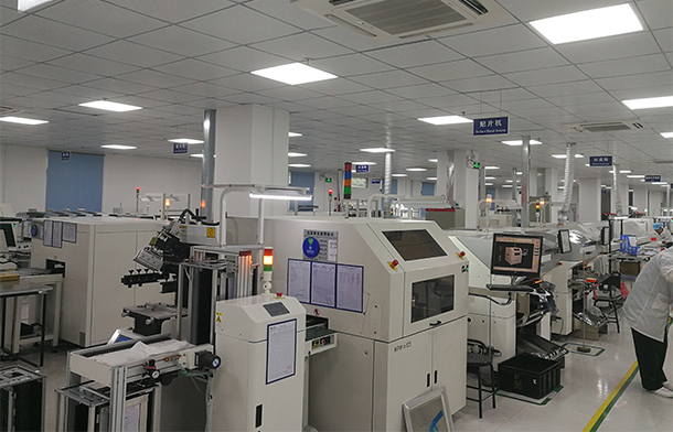
Circuit Board Fabrication and PCB Assembly Turnkey Services
Metal core PCB asked questions
What are metal core PCBs used for
What are the advantages of metal core PCBs?
What are the different types of metal core materials available?
How do I select a metal core PCB manufacturer?
Can metal core PCBs be repaired or modified?
The delivered assembled PCBs worked flawlessly. The component placement is superb. Mis wang, the WINOW engineer in charge of our project, and I clicked immediately. She asked pertinent questions to ensure the project was completed correctly. We had a pleasant, brief, and to-the-point conversation.
This board is required to charge the lipo batteries on my robotic platform (rover). For a first-time order, there was excellent communication throughout the ordering process, manufacturing progress, and delivery tracking. Very reasonable price, especially for the first order with a discount credit.
Yesterday, the boards arrived, and assembly has begun. Excellent solder wetting, crisp line definition, and drill holes that are precisely centered on via lands. Please convey my gratitude to everyone who created such wonderful boards.
Why Choose Us?
WINOW has been providing high-quality PCBs with quick turnaround times and high customer satisfaction since 2018. We are one of China's largest and most skilled board manufacturers.
-
 Prototype orders are processed within 24 hours.
-
The lead time for small batch production and some PCB prototypes is 48 hours.
-
Typically, PCB prototypes and small-batch manufacturing take 5-7 working days.
Quick payment
Flexible payment options
On-Demand Manufacturing
There is no minimum purchase or order amount. Orders for prototypes and mass production are both accepted.
Inspection Of Quality
90% of the technical staff has more than ten years of experience in the industry
Technical Strength
PCB Assembly can be adjusted at any time to meet customer ICT, veneer, aging, and ATE requirements.