

PCB FAI
FAI (First Article Inspection) is a quality control process that involves verifying that the first production run of a product or component meets the specified design and quality standards. It is commonly used in the electronics manufacturing industry to ensure that the production process is working correctly and that the finished product meets the required specifications.
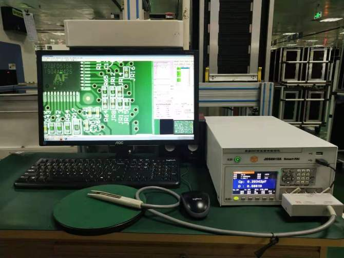
In the context of PCB (printed circuit board) manufacturing, FAI typically involves comparing the actual PCB to the design documents and verifying that it meets all of the specified requirements. This may include visual inspection, dimensional measurement, and functional testing.
There are several benefits to performing FAI on PCBs:
- Improved product quality: By identifying and correcting defects early in the manufacturing process, FAI can help improve the overall quality of the finished product.
- Reduced rework and scrap: By catching defects early, FAI can reduce the need for rework and scrap, which can save time and reduce costs.
- Improved process control: FAI can help identify and correct issues with the manufacturing process, which can improve process control and reduce the risk of future defects.
However, there are also some limitations to FAI:
- Cost: FAI requires additional time and resources, which can increase the overall cost of the manufacturing process.
- Dependence on human inspection: FAI typically involves manual inspection, which can be subject to human error.
- Limited to the first production run: FAI is only performed on the first production run, so defects that occur in subsequent runs may not be detected.
PCB FAI FAQ
- What is FAI (First Article Inspection)?
FAI (First Article Inspection) is a quality control process that involves verifying that the first production run of a product or component meets the specified design and quality standards. It is commonly used in the electronics manufacturing industry to ensure that the production process is working correctly and that the finished product meets the required specifications.
- What is the purpose of FAI in PCB manufacturing?
In the context of PCB (printed circuit board) manufacturing, FAI typically involves comparing the actual PCB to the design documents and verifying that it meets all of the specified requirements. This may include visual inspection, dimensional measurement, and functional testing.
- What are the benefits of performing FAI on PCBs?
There are several benefits to performing FAI on PCBs:
- Improved product quality: By identifying and correcting defects early in the manufacturing process, FAI can help improve the overall quality of the finished product.
- Reduced rework and scrap: By catching defects early, FAI can reduce the need for rework and scrap, which can save time and reduce costs.
- Improved process control: FAI can help identify and correct issues with the manufacturing process, which can improve process control and reduce the risk of future defects.
- What are the limitations of FAI?
There are a few limitations to FAI:
- Cost: FAI requires additional time and resources, which can increase the overall cost of the manufacturing process.
- Dependence on human inspection: FAI typically involves manual inspection, which can be subject to human error.
- Limited to the first production run: FAI is only performed on the first production run, so defects that occur in subsequent runs may not be detected.
- How is FAI typically performed?
FAI typically involves comparing the actual product or component to the design documents and verifying that it meets all of the specified requirements. This may include visual inspection, dimensional measurement, and functional testing. In some cases, additional testing or analysis may be required to verify that the product meets the specified requirements.