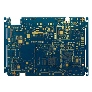
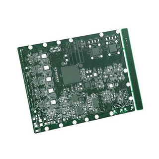
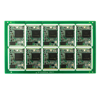
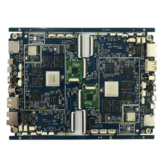
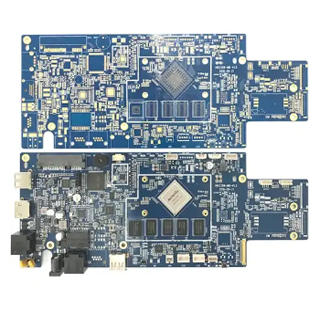
Multilayer PCB
-
Supplier Type: PCB Fabrication
-
Material: KB6061,S1141,S1000,IT180
-
Plate thlCkness: 1.6mm
-
Minimum aperture: 0.296mm
-
Line width: 0.342*0.37mm
-
Size: 43.68*38.9mm
- No MOQ or MPQ limited.
- Daily quotes and negotiations.
- Prototypes quotation within 3h.
- Flexible payment options.
- Prototype or mass production order acceptable.
-
Project Info
-
Specification
What are Multilayer PCBs?
Multilayer printed circuit boards are made up of numerous layers of conducting material and insulating material. They are more dense, flexible, and more efficient designs than single-layer PCBs. Multilayer PCBs are utilized in various applications, including computers, cell phones, automotive systems, and medical equipment.
A multilayer PCB might have anywhere from 4 to 40 layers or more. The more layers there are on a PCB, the more difficult and expensive it is to design and build. The complexity of the circuit and the intended performance define the number of layers in a multilayer PCB.
Benefits of Multilayer PCBs
Multilayer PCBs have numerous advantages over single-layer PCBs. For starters, multilayer PCBs provide greater circuit density and flexibility. You may fit more components in a smaller area by using multiple layers. This enables more efficient and dependable designs.
Multilayer printed circuit boards also provide better signal integrity and electrical performance. When compared to single-layer PCBs, utilizing many layers reduces crosstalk and interference. As a result, signal integrity and performance are improved.
Multilayer PCBs also provides better heat control. You can improve the thermal qualities of the board by employing numerous layers. This can result in increased cooling and reliability.
Finally, multilayer PCBs provide more design flexibility. You can move components around on various layers to optimize the layout and performance of the board. This can lead to better performance and dependability.
Multilayer PCB Design Process
The design procedure for multilayer PCBs is identical to that of single-layer PCBs. The first step is to create a schematic diagram of the circuit. This allows you to see the components and connections on the board.
The next step is to create a component placement diagram. This allows you to place the components on the board more efficiently. By optimizing the board’s layout, you can also improve its performance and dependability.
The next step is to create a route diagram. This assists you in determining the best route to link the components by routing the traces. This is a critical step in improving the board’s performance.
The last step is to make a gerber file. This is a file containing all of the information required to make the board. It contains information about component placement, routing, vias, and other features. This is the file that is used to create the PCB.
Multilayer PCB Materials
Materials of many sorts are used in the production of multilayer PCBs. FR-4, polyimide, and high-temperature epoxy are the most commonly used materials.
The most prevalent material used in multilayer PCBs is FR-4. It is a sturdy and long-lasting fiberglass-reinforced epoxy laminate.
Polyimide is a flexible material that is commonly used in flexible printed circuit boards. Because of its flexibility and great temperature resistance, it is widely employed.
A material used in high-temperature applications is high-temperature epoxy. It costs more than FR-4 and polyimide but has better thermal tolerance.
Multilayer PCB Manufacturing Process
Multilayer PCBs are manufactured in the same way as single-layer PCBs. The first step is to use the Gerber file to design the PCB. This is accomplished through the use of a technique known as photolithography. This is the process of exposing a photosensitive material to light and then etching it to form the traces and other characteristics of the board.
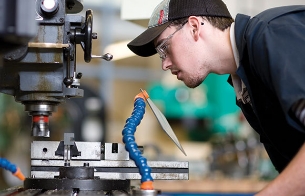
The vias will be drilled next. The holes that connect the different layers of the board are known as vias. A CNC machine is used to drill them.
The solder mask and silkscreen will be applied next. The solder mask is a protective layer that is put to the board to keep it from oxidizing and becoming contaminated with other pollutants. The silkscreen is a printed legend that indicates the board’s components and connections.
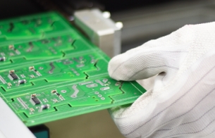
The final step is to put the pieces together. This can be done manually or using a pick-and-place machine. The board is then tested for functionality after the components are soldered to it.
Multilayer PCB Design Considerations
There are various factors to consider while constructing a multilayer PCB.
The first factor to examine is the number of layers. The number of layers in a PCB is decided by the complexity of the circuit and the intended performance, as previously stated. It is critical to determine the number of layers required for the desired performance.
The thickness of the board is the second factor to consider. The thickness of the board will affect its electrical performance. It is critical to determine the thickness required for the desired performance.
The third factor to examine is the trace width and spacing. The current carried by the traces determines the breadth and spacing of the traces. It is critical to calculate the required trace width and spacing for the desired performance.
The fourth factor to examine is the copper weight. The copper weight represents the amount of copper on the board. It is critical to determine the copper weight required for the desired performance.
Finally, the final factor to examine is thermal management. Thermal management on the board is critical for dependable and efficient functioning. It is critical to identify the thermal management required for the desired performance.
Multilayer PCB Troubleshooting
When troubleshooting a multilayer PCB, numerous methods can be performed to detect and fix the problem.
The first step is to double-check the schematic for mistakes. This can be accomplished by comparing the schematic to the datasheet for each component. This will aid in identifying any mistakes in the schematic.
The second step is to double-check the layout for mistakes. This can be accomplished by visually reviewing the board or by utilizing a layout tool. This will aid in identifying any flaws in the layout.
Checking the connections is the third stage. This can be accomplished by visually analyzing the board or by utilizing a continuity tester. This will aid in identifying any mistakes in the connections.
The fourth stage is to inspect the parts. This can be accomplished by visually checking the components or by using a multimeter. This will aid in identifying any flaws in the components.
The fifth step is to inspect the power source. This can be accomplished by visually examining the power supply or by using a multimeter. This will aid in identifying any problems with the power supply.
Advantages and Disadvantages of Multilayer PCBs
Multilayer printed circuit boards have numerous advantages over single-layer printed circuit boards. They provide enhanced circuit density and flexibility, better signal integrity and electrical performance, better thermal management, and more design flexibility.
However, multilayer PCBs have several drawbacks. They are more expensive and difficult to design and produce than single-layer PCBs. They also necessitate more specialized assembling and testing equipment.
Conclusion
Multilayer PCBs are an excellent approach to transforming your designs. They have numerous advantages over single-layer PCBs, including higher circuit density and flexibility, improved signal integrity and electrical performance, improved heat management, and greater design flexibility.
Multilayer PCBs are the way to go if you want to take your designs to the next level. They have numerous benefits and might assist you in developing more effective and dependable designs.
So, what are you holding out for? Begin exploring the world of multilayer PCBs today and transform your designs!
Basic introduction
| Name: | Multilayer PCB |
| Material:: | KB6061,S1141,S1000,IT180 |
| Application | Automotive industry, Power supplies and power converters, Welding equipment |
| Electrical Testing | Fixture / Flying Probe |
| Quality Grade | Ipc Class 2, Ipc Class 3 |
| Silkscreen Colors | Red Oil/Green/Blue/Black/White |
| Other Testing | Aoi, X-ray(Au&Ni), Controlled Impedance Test |
| Placement speed: | Chip component placement speed (at best conditions) 0.036 S/piece |
| Surface Finishes | Immersion Gold, OSP, and HASL |

Our 2 Layer PCB Board Features
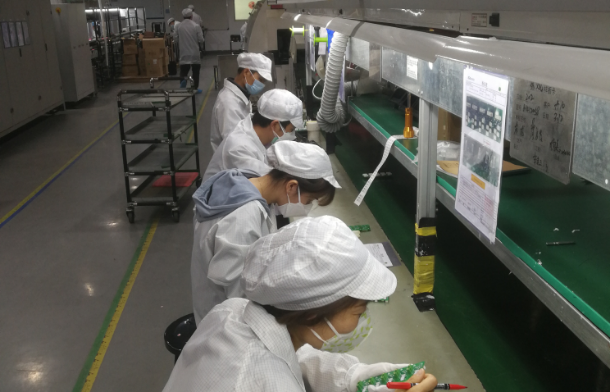
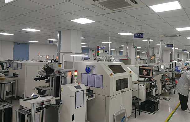
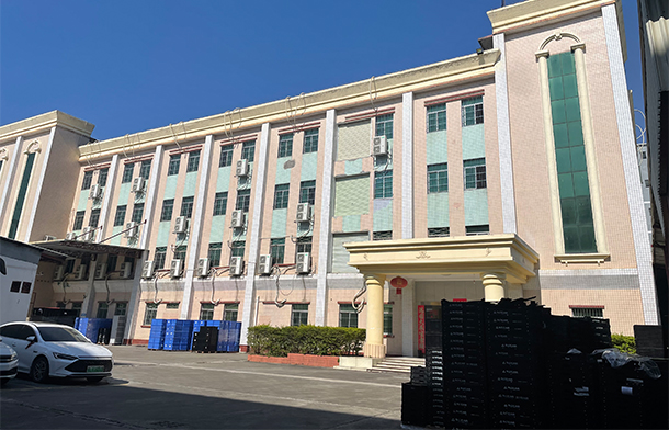
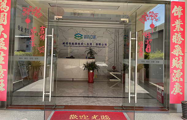
Our PCB Factory Tour

Why choose us for PCB assembly services
Economy
We can provide various types of PCB boards and various materials at competitive prices according to customer requirements.
Best Team
No Matter What Kind Of Pcb Board You Want, Our Trained Designers Can Make lt lnAbout 10-12 Working Days. Emplovees Know The lmportance Of Deadlines, AndTheir Goal ls To Give You Top-Notch Results Within A Specified Time Frame.
Best Team
No Matter What Kind Of Pcb Board You Want, Our Trained Designers Can Make lt lnAbout 10-12 Working Days. Emplovees Know The lmportance Of Deadlines, AndTheir Goal ls To Give You Top-Notch Results Within A Specified Time Frame.
Service
Brnon co0p PchaSn To Functes Candackage Finish , We Provid