

PCB Assembly Definition: Understanding the Basics
PCB assembly is a fundamental process in the production of electronic devices. It involves the assembly of various electronic components onto a printed circuit board (PCB) to create a functional electronic device. PCB assembly definition refers to the process of assembling these components onto the PCB, which requires a range of specialized equipment and techniques.
The PCB assembly process involves several stages, including component placement, soldering, and inspection. Component placement involves the precise placement of electronic components onto the PCB, which is typically done using automated equipment. Soldering is the process of bonding the components to the PCB using soldering techniques, such as wave soldering or reflow soldering. Inspection is performed to ensure that the components are correctly placed and soldered, and that the PCB is functioning as expected.
PCB assembly definition is critical in the production of electronic devices, as it directly impacts the quality and functionality of the final product. The process requires specialized knowledge and expertise, and must be performed with great care and attention to detail. As electronic devices continue to become more complex and sophisticated, the importance of PCB assembly in the manufacturing process will only continue to grow.
Basics of PCB Assembly
Components of a PCB
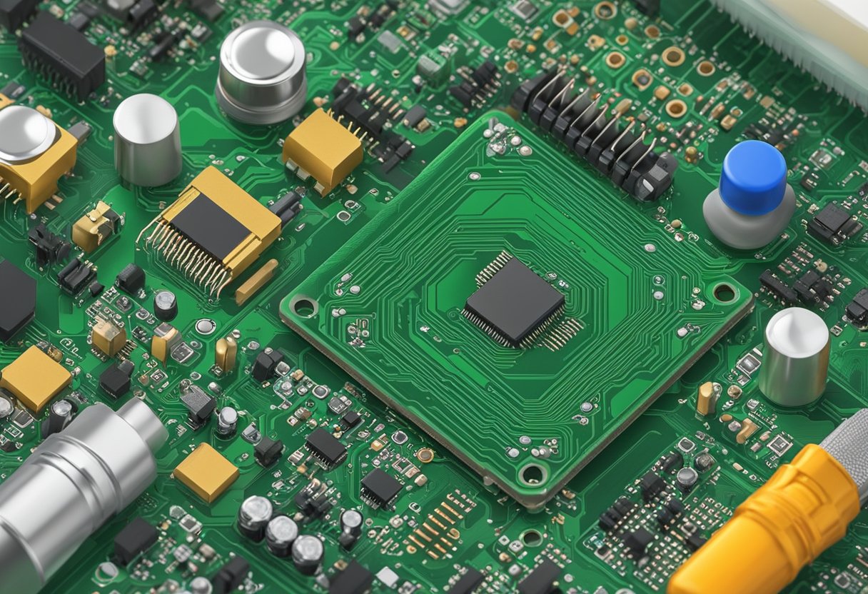
A Printed Circuit Board (PCB) is a board made of insulating material with conductive pathways etched onto its surface. It is used to connect various electronic components together. The components of a PCB include resistors, capacitors, diodes, transistors, and integrated circuits. These components are attached to the PCB through soldering.
PCB Assembly Process
PCB assembly is the process of attaching electronic components to a PCB. This process involves several steps, including:
- Solder Paste Application: Solder paste is applied to the PCB using a stencil. This paste is a mixture of small metal balls and flux.
- Pick and Place: The electronic components are picked up by a machine and placed on the PCB in their proper locations.
- Reflow Soldering: The PCB is heated to a high temperature to melt the solder paste and create a permanent connection between the components and the PCB.
- Inspection: The PCB is inspected to ensure that all the components are properly attached and that there are no defects.
- Testing: The PCB is tested to ensure that it is functioning properly.
Overall, the PCB assembly process is a crucial step in the production of electronic devices. It requires precision and attention to detail to ensure that the final product is of high quality.
Types of PCB Assembly
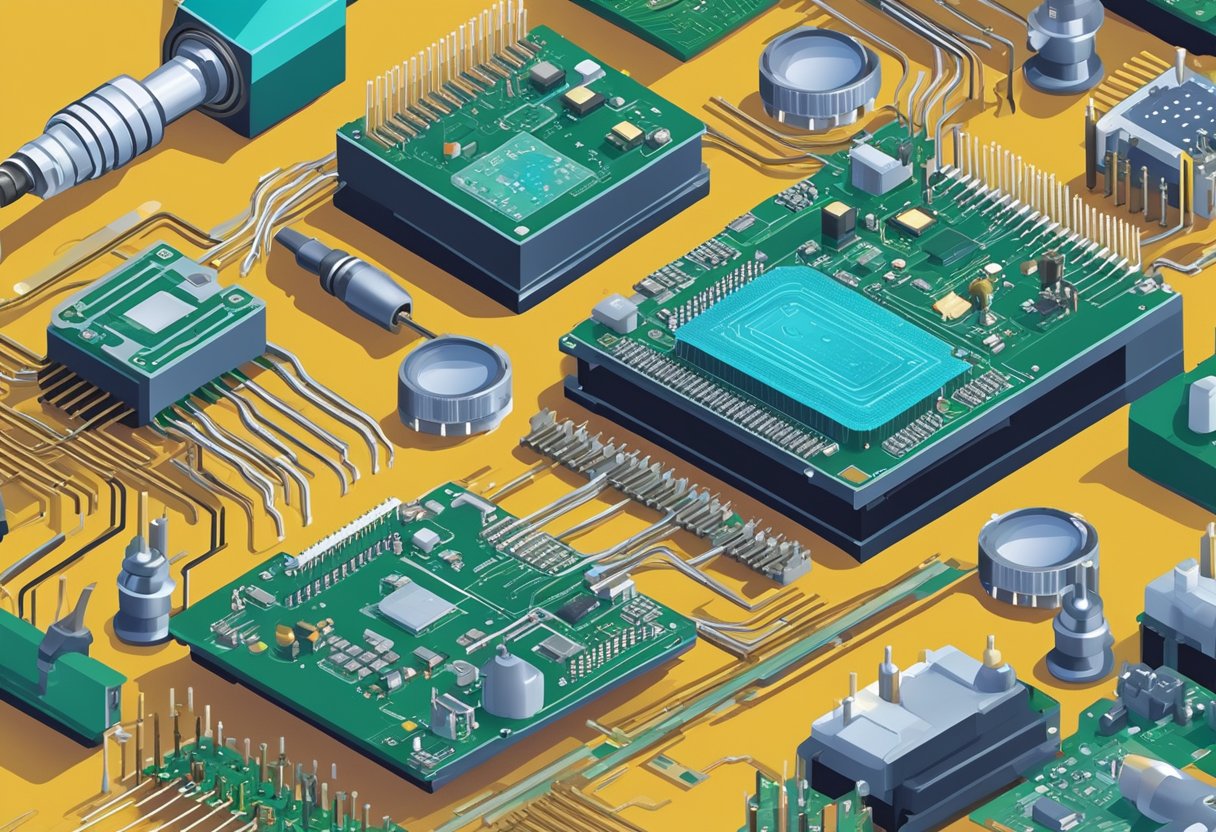
There are different types of PCB assembly technologies available that are used in different applications. The most common types of PCB assembly include through-hole technology, surface-mount technology, and mixed technology PCB assembly.
Through-Hole Technology
Through-hole technology is the oldest and most traditional method of PCB assembly. It involves drilling holes into the PCB and inserting components through the holes. The components are then soldered onto the board from the other side. Through-hole technology is commonly used for components that require a high level of mechanical stability, such as large capacitors, transformers, and power transistors.
Surface-Mount Technology
Surface-mount technology (SMT) is a newer method of PCB assembly that involves mounting components directly onto the surface of the PCB. This method eliminates the need for drilling holes, which makes the PCB smaller and lighter. SMT components are usually smaller and lighter than through-hole components, which makes them ideal for high-density applications. SMT is commonly used for components such as resistors, capacitors, and integrated circuits.
Mixed Technology PCB Assembly
Mixed technology PCB assembly is a combination of through-hole and surface-mount technologies. This method is used when a PCB requires both through-hole and surface-mount components. Mixed technology PCB assembly can be more complex than other methods because it requires both types of components to be mounted on the same board. However, it is often the best choice when a PCB requires a mix of high-power and high-density components.
In conclusion, the type of PCB assembly technology used depends on the requirements of the specific application. Each method has its own advantages and disadvantages, and the choice of method should be based on the specific needs of the project.
Design Considerations for PCB Assembly
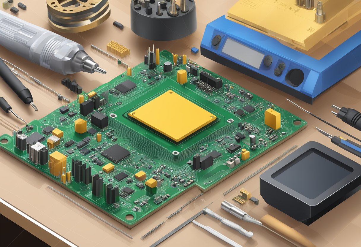
When designing a PCB assembly, there are several considerations that must be taken into account to ensure that the final product is functional and reliable. This section will cover some of the most important design considerations for PCB assembly, including material selection, component placement, and thermal management.
Material Selection
The choice of materials used in PCB assembly can have a significant impact on the performance and reliability of the final product. The most common materials used in PCB assembly include FR-4, polyimide, and ceramic. FR-4 is the most widely used material due to its low cost and good electrical properties. Polyimide is used for flexible circuits, while ceramic is used for high-temperature applications.
When selecting materials for PCB assembly, designers must consider factors such as the operating environment, the electrical properties required, and the cost of the materials. It is also important to ensure that the chosen materials are compatible with the manufacturing process being used.
Component Placement
The placement of components on a PCB is another important consideration in PCB assembly. Components must be placed in such a way that they can be easily accessed for assembly, testing, and repair. They must also be placed in a way that minimizes the length of the traces between them, reducing the risk of interference and signal degradation.
When placing components on a PCB, designers must consider factors such as the size and shape of the components, the location of connectors and other interface points, and the overall size and shape of the PCB.
Thermal Management
Thermal management is a critical consideration in PCB assembly, as excess heat can damage components and reduce the lifespan of the product. To manage heat, designers must ensure that the PCB has adequate ventilation and that heat-generating components are placed in areas where they can dissipate heat effectively.
Other thermal management techniques that can be used in PCB assembly include the use of heat sinks, thermal vias, and thermal pads. These techniques can help to reduce the temperature of critical components and ensure that the product operates reliably over its expected lifespan.
In summary, when designing a PCB assembly, designers must consider a range of factors to ensure that the final product is functional, reliable, and cost-effective. Material selection, component placement, and thermal management are three of the most important considerations in PCB assembly, and must be carefully managed to ensure that the final product meets the required specifications.
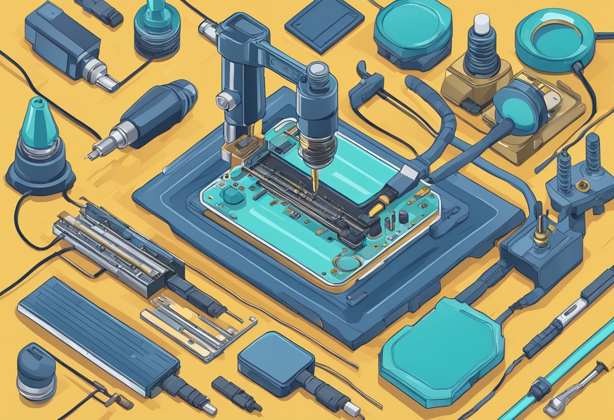
PCB Assembly Equipment
PCB assembly equipment is a crucial part of the manufacturing process for printed circuit boards. This equipment is used to place and solder electronic components onto the board. The following subsections describe some of the most commonly used types of equipment.
Pick-and-Place Machines
Pick-and-place machines are used to accurately place electronic components onto a PCB. These machines use a combination of mechanical and vacuum systems to pick up components from a feeder and place them onto the board. Pick-and-place machines can place components of various sizes and shapes, including surface-mount components. They are capable of placing hundreds of components per minute, making them a crucial part of the PCB manufacturing process.
Soldering Equipment
Soldering equipment is used to attach electronic components to the PCB by melting solder and creating a bond between the component and the board. There are several types of soldering equipment, including wave soldering machines, reflow ovens, and hand-held soldering irons. Wave soldering machines are used for through-hole components, while reflow ovens are used for surface-mount components. Hand-held soldering irons are used for manual soldering of components that cannot be placed by pick-and-place machines.
Inspection and Testing Equipment
Inspection and testing equipment is used to ensure that the PCB has been manufactured correctly and that all components are functioning properly. This equipment includes automated optical inspection (AOI) machines, X-ray machines, and in-circuit testers (ICTs). AOI machines inspect the board for defects such as missing components, incorrect component placement, and solder defects. X-ray machines are used to inspect the internal structure of components and the solder joints. ICTs test the functionality of the components on the board.
In conclusion, PCB assembly equipment is an essential part of the PCB manufacturing process. The equipment described above is used to place and solder electronic components onto the board, and to inspect and test the board for defects. The use of this equipment ensures that the PCB is manufactured correctly and that all components are functioning properly.
Soldering Techniques in PCB Assembly
Wave Soldering
Wave soldering is a technique used in PCB assembly where the PCB is passed over a wave of molten solder. The wave is created by a pump that pumps molten solder from a reservoir onto a wave-making device. The PCB is then passed over the wave, and the solder is deposited onto the PCB.
Wave soldering is a fast and efficient way to solder large numbers of PCBs. It is often used in high-volume manufacturing environments where speed and efficiency are critical. However, it is not suitable for all types of PCBs, and it can be difficult to control the amount of solder that is deposited onto the PCB.
Reflow Soldering
Reflow soldering is a technique used in PCB assembly where the solder is melted using heat. The solder is applied to the PCB in the form of a paste, which contains a mixture of solder and flux. The PCB is then heated to a temperature that melts the solder, causing it to flow and bond to the PCB.
Reflow soldering is a popular technique because it is versatile and can be used to solder a wide range of components, including surface-mount components. It is also relatively easy to control the amount of solder that is deposited onto the PCB. However, it can be more time-consuming than wave soldering, and it requires more equipment and expertise.
In conclusion, both wave soldering and reflow soldering are important techniques in PCB assembly. The choice of technique depends on a variety of factors, including the type of PCB, the volume of production, and the desired level of control over the soldering process. By understanding the advantages and limitations of each technique, PCB assemblers can choose the most appropriate technique for their specific needs.