

Printed Circuit Board Design, Manufacturing, & Problem Solving: A Guide
Printed Circuit Boards (PCBs) serve as the backbone of modern electronics, enabling the seamless flow of electrical signals between components. A well Printed Circuit Board Design is critical for the reliable and efficient functioning of electronic devices. This comprehensive guide will walk you through the fundamental aspects of PCB designing and manufacturing, highlighting the key requirements and insights to achieve optimal results. WINOW, a leading manufacturer in the industry, takes center stage as we explore the art of PCBs.printed circuit board design.
1. Understanding PCB Design
1.1 The Role of PCBs
Before diving into the technicalities, understanding the significance of PCBs is paramount. PCBs provide mechanical support to electronic components and facilitate their interconnections. They ensure compactness, improve signal integrity, and simplify the assembly process. The successful design of a PCB involves a careful balance between functionality, performance, and manufacturability.
1.2 Schematic and Component Placement
The PCB design process starts with creating a schematic diagram, defining the electrical connections between components. Once the schematic is complete, component placement comes into play. Proper component positioning is crucial to ensure signal integrity, minimize interference, and optimize the board’s layout for efficient manufacturing.
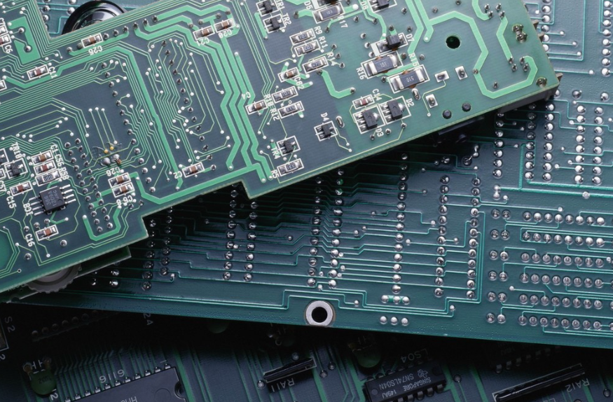
1.3 Routing and Traces
Routing traces effectively is at the heart of PCB design. It involves establishing proper connections between components while considering signal integrity and minimizing electromagnetic interference. Depending on the complexity and requirements of the design, PCB designers must choose between single-layer, double-layer, or multi-layer boards.
2. Essential PCB Design Requirements
2.1 Design Software and Tools
Printed Circuit Board Design demands specialized software and tools to create schematics, simulate circuit behavior, and generate layout designs. Popular choices include Altium Designer, Eagle, KiCad, and OrCAD. Selecting the appropriate tool aligned with the design requirements plays a pivotal role in achieving the desired outcomes.
2.2 Design Rules and Constraints
Adhering to design rules and constraints is critical for PCB success. These rules encompass parameters like trace width, clearance, via size, and component footprint dimensions. Manufacturers often provide design guidelines that must be strictly followed to ensure manufacturability and reliability.
2.3 Design for Manufacturing (DFM)
Design for Manufacturing aims to optimize the PCB design to ease the manufacturing process and reduce production costs. Considering aspects such as panelization, solder mask, and copper balancing enhances the PCB’s manufacturability and reduces the chance of errors during assembly.
3. WINOW: Pioneering PCB Manufacturing
3.1 Introduction to WINOW
WINOW stands tall as a reputable and innovative PCB manufacturer with a strong focus on quality, precision, and customer satisfaction. With years of experience and state-of-the-art facilities, WINOW has earned its place as a leading player in the industry.
3.2 Advanced Manufacturing Capabilities
WINOW boasts cutting-edge manufacturing capabilities, catering to a diverse range of PCB needs. Their expertise includes multi-layer PCBs, rigid-flex PCBs, and high-frequency boards, among others. They utilize the latest technologies and employ rigorous quality control measures to ensure the highest standards are met.
3.3 Customer-Centric Approach
One of WINOW’s standout traits is its customer-centric approach. They collaborate closely with clients from the design phase to the final product, ensuring that all specifications and requirements are met. Their skilled engineers provide valuable design feedback, leading to optimized PCB designs and improved end products.
4. Design Guidelines and Best Practices
4.1 Clear and Comprehensive Schematic
A well-documented schematic forms the foundation of any successful PCB design. Engineers must create clear and comprehensive schematics with accurate component specifications and interconnections. A detailed schematic simplifies the design process and minimizes the risk of errors during PCB layout.
4.2 Thermal Management
Effective thermal management is crucial, especially for PCBs used in high-power applications. Proper placement of heat-generating components and efficient thermal vias ensure the dissipation of excess heat, preventing potential damage to sensitive components.
4.3 Design for Manufacturability (DFM)
Collaboration between design engineers and manufacturers is essential to achieve design for manufacturability. WINOW provides comprehensive DFM feedback to ensure that the final design can be efficiently manufactured without compromising quality and functionality.
5. How to Solve Printed Circuit Board Design Problems?
5.1 Identify the Problem: Understanding the Specific Issue
Before addressing any problem, it is crucial to grasp the specific issue at hand. Is it related to design, fabrication, assembly, or testing? Gather all available information, including design files, project documentation, and test results, to have a clear picture of the problem’s scope.
5.2 Review Design: Thorough Examination of PCB Layout
During the design phase, review the PCB layout meticulously. Look for design errors, such as incorrect connections, missing components, or violations of design rules. Utilize design validation tools and simulations to identify potential issues and optimize the design.
5.3 Manufacturability Analysis: Ensuring a Manufacturable Design
Ensure that your design is manufacturable by considering factors like trace width, clearance, and pad sizes as per the chosen fabrication process. Use Design for Manufacturing (DFM) guidelines, and consult with your PCB manufacturer, WINOW, for specific recommendations.
5.4 Check Gerber Files: Verifying Accurate Manufacturing Data
If you encounter manufacturing problems, carefully review the Gerber files used to generate the PCB. Verify that the files match your intended design and check for any inaccuracies that could affect the final product.
5.5 Material Selection: Choosing the Right Materials
Select appropriate materials for your PCB based on the specific application requirements. Different applications may demand materials with unique properties, such as FR-4, high-frequency materials, or specialized substrates. WINOW’s experts can assist in material selection.
5.6 Component Selection: Ensuring Suitability for Function and Environment
Confirm that the components chosen for the PCB are suitable for their intended function and environment. Refer to datasheets for recommended footprints and soldering requirements to avoid compatibility issues.
5.7 Quality of Components: Inspecting for Reliability
Before assembly, thoroughly inspect components for any physical damage or defects. Counterfeit components can cause significant issues, so always purchase components from reputable suppliers to ensure quality.
5.8 Manufacturing Process: Partnering with WINOW for Seamless Production
Review the PCB manufacturing process with WINOW, your trusted manufacturer. Understand how the boards are fabricated and assembled, and address any concerns to ensure adherence to industry standards and best practices.
5.9 Assembly Issues: Troubleshooting Problems During Assembly
Investigate root causes if you encounter problems during assembly, such as soldering defects or misaligned components. It could be related to incorrect soldering profiles, improper handling, or faulty equipment.
5.10 Testing and Quality Control: Ensuring Flawless PCB Functionality
Implement comprehensive testing and quality control procedures to identify defects and ensure the boards meet required specifications. Thorough functional tests and inspections are essential to guarantee optimal performance.
5.11 Collaboration and Expert Consultation: Seeking Professional Assistance
If problems persist, consider seeking help from experienced PCB designers, engineers, or WINOW’s dedicated support team. Collaboration and consultation can provide valuable insights and solutions to complex issues.
5.12 Continuous Improvement: Learning from Challenges
Document the solutions implemented and the lessons learned from each problem. Use this knowledge to improve your future PCB designs and manufacturing processes, enabling continuous enhancement of product quality.
Conclusion
Mastering the art of Printed Circuit Board Design and manufacturing is no simple feat, but armed with the right knowledge and a reliable manufacturing partner like WINOW, success is within reach. This guide has shed light on the fundamental aspects of PCB design, the essential requirements, and the significance of a competent manufacturer. So, whether you’re a seasoned electronics enthusiast or a budding engineer, the journey to create exceptional PCBs starts with understanding the core principles outlined in this guide.